SS9012
High-gain, high-speed switching transistor for a variety of application
Inventory:6,804
- 90-day after-sales guarantee
- 365 Days Quality Guarantee
- Genuine Product Guarantee
- 7*24 hours service quarantee
-
Part Number : SS9012
-
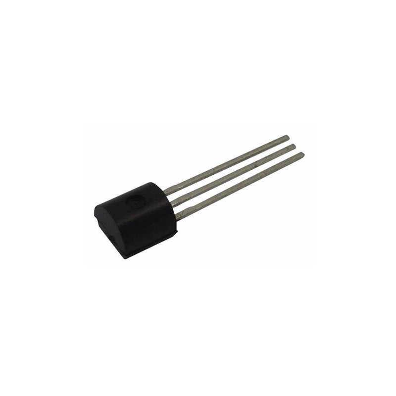
Package/Case : TO-92-3
-
Brands : FAIRCHILD/ON
-
Components Categories : Single Bipolar Transistors
-
Datesheet : SS9012 DataSheet (PDF)
Overview of SS9012
1W Output Amplifier of Potable Radios in Class B Push-pull Operation. • High total power dissipation. (PT=625mW)• High Collector Current. (IC= -500mA)• Complementary to SS9013• Excellent hFE linearity.
Key Features
- High Total Power Dissipation: (PT = 625mW)
- High Collector Current : (IC=-500mA)
- Complementary to SS9013
- Excellent hFElinearity.1W Output Amplifier of Portable Radios in Class B Push-pull Operation.
Application
- This item is very flexible.
- Great for many different uses.
- Adaptable to diverse situations.
Specifications
The followings are basic parameters of the part selected concerning the characteristics of the part and categories it belongs to.
| Product Category | Bipolar Transistors - BJT | Mounting Style | Through Hole |
| Package / Case | TO-92-3 | Transistor Polarity | PNP |
| Configuration | Single | Collector- Emitter Voltage VCEO Max | 20 V |
| Collector- Base Voltage VCBO | 40 V | Emitter- Base Voltage VEBO | 5 V |
| Maximum DC Collector Current | 500 mA | Pd - Power Dissipation | 625 mW |
| Minimum Operating Temperature | - 55 C | Maximum Operating Temperature | + 150 C |
| Series | SS9012 | Brand | onsemi / Fairchild |
| Continuous Collector Current | 500 mA | DC Collector/Base Gain hfe Min | 64 |
| DC Current Gain hFE Max | 202 | Height | 4.58 mm |
| Length | 4.58 mm | Product Type | BJTs - Bipolar Transistors |
| Subcategory | Transistors | Technology | Si |
| Width | 3.86 mm | Unit Weight | 0.008466 oz |
Warranty & Returns
Warranty, Returns, and Additional Information
-
QA & Return Policy
Parts Quality Guarantee: 365 days
Returns for refund: within 90 days
Returns for Exchange: within 90 days
-
Shipping and Package
Shipping:For example, FedEx, SF, UPS, or DHL.UPS, or DHL.
Parts Packaging Guarantee: Featuring 100% ESD anti-static protection, our packaging incorporates high toughness and superior buffering capabilities.
-
Payment
For example, channels like VISA, MasterCard, UnionPay, Western Union, PayPal, and more.
If you have specific payment channel preferences or requirements, please get in touch with our sales team for assistance.
Similar Product

FGH40N60UFD
High-power transistor for industrial applicatio

FDV302P
Trans MOSFET P-CH 25V 0.12A 3-Pin SOT-23 T/R

FQPF2N60C
Trans MOSFET N-CH 600V 2A 3-Pin(3+Tab) TO-220FP Tube

FDS8880
Trans MOSFET N-CH 30V 11.6A 8-Pin SOIC T/R

KSP94TA
The KSP94TA transistor is a TO-92-packaged PNP type with a voltage rating of 400V and a current rating of 0

FQPF13N06L
60V N-Channel QFET Logic Level MOSFET FQPF13N06L

FCA76N60N
TO-3PN-3 MOSFETs that meet ROHS requirements

FDD6612A
High-performance power electronic component for efficient energy conversi
