The Ultimate Guide to MOS Tube: Function, Application, Advantage & Three Poles
 Dr. James Anderson
Published:February 26, 2024
The history of MOS Tubes dates back to the 1960s when they were first developed as a replacement for bipolar junction transistors (BJTs). Over the years, MOS Tubes have undergone significant advancements, leading to improved performance, reliability, and efficiency. Today, they are widely used in a wide range of applications, from integrated circuits to power electronics. MOS Tubes play a vital role in modern electronics due to their unique characteristics, such as high input resistance, low power consumption, and fast switching speeds. They are used in various applications, including digital logic circuits, memory devices, amplifiers, and voltage regulators. Their importance in the field of electronics continues to grow as new technologies and applications emerge. In this article, we'll explore what is MOS tube. Delve into its characteristics, function, advantage, application and how to choose the right MOS tube, etc.

What is MOS Tube?
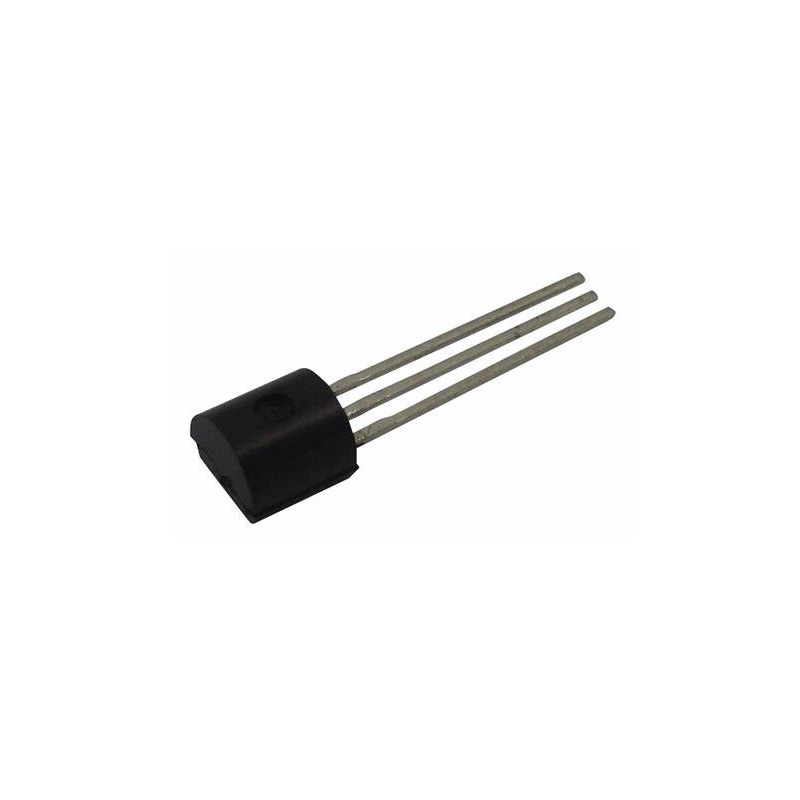
The mos tube is a MOSFET(metal-oxide-semiconductor field-effect transistor), or a metal-insulator-semiconductor, features a structure where the source and drain can be interchanged. These regions are N-type, situated within the P-type backgate. Even if the source and drain are reversed, the device's performance remains unaffected, rendering it symmetrical.
In contrast, a bipolar transistor amplifies a small input current change into a larger output current change. Its gain, defined as the ratio of output to input current (beta), characterizes its performance. On the other hand, a field-effect transistor (FET) translates input voltage changes into output current changes. The FET's gain, or transconductance, represents the ratio of output current change to input voltage change. Common types in the market include N-channel and P-channel FETs. For specific illustrations, see the image on the right (depicting an N-channel depletion MOS transistor). The typical P-channel variant is a low-voltage MOSFET.
The FET modulates transistor current flow by generating an electric field across an insulating layer. No actual current flows through this insulator, resulting in minimal GATE current in the FET. Most FETs utilize a thin silicon dioxide layer as an insulator beneath the GATE terminal. Such transistors are known as metal-oxide-semiconductor (MOS) transistors, or MOSFETs. Due to their smaller size and higher efficiency, MOSFETs have supplanted bipolar transistors in numerous applications.

Internal Structure of MOS Tube
Types and Structures of MOS Tube
MOSFET, or Metal-Oxide-Semiconductor Field-Effect Transistor, represents a type of FET (Field-Effect Transistor), alongside JFET (Junction Field-Effect Transistor). MOSFETs can be fabricated in various configurations, including enhancement or depletion types, and as either P-channel or N-channel devices. However, in practical applications, only the enhancement-type N-channel MOS transistor and enhancement-type P-channel MOS transistor are typically needed, hence the common references to NMOS or PMOS.
The rationale for not using depletion MOS transistors is not usually explained. Among the two enhancement MOS transistors, NMOS is more prevalent due to its lower on-resistance and simpler manufacturing process. Consequently, NMOS is commonly employed in applications such as switching power supplies and motor drives. Subsequently, this discussion will primarily focus on NMOS.
Parasitic capacitance naturally exists between the three terminals of a MOS transistor, despite not being desired. This capacitance arises from manufacturing processes and, while it complicates driving circuit design or selection, it is an unavoidable characteristic that will be further detailed later.
The schematic diagram of a MOS transistor reveals the presence of a parasitic diode between the drain and the source. This diode plays a critical role in driving appropriate loads. Additionally, it's worth noting that the body diode is unique to single metal oxide semiconductor transistors and is typically absent in integrated circuit chips.

MOS Tube Working Principle
The MOS tube, or metal oxide semiconductor field-effect transistor, operates based on the distinct conducting properties of diffusion current and electric field in the vertical direction between the p-type area beneath the insulated gate and the source-drain. Let’s take N-channel enhanced type as an example.

Schematic Diagram of the Structure of N-channel Enhancement Mode MOS Transistor

(1) When VGS = 0, regardless of the polarity of VDS, there is always a reverse-biased PN junction, resulting in no conductive channel. Therefore, ID = 0 when VGS = 0. The MOSFET can only operate when VGS is greater than 0.

(2) When VGS is greater than 0, an electric field perpendicular to the semiconductor surface is created in the SiO2 medium. This field repels the majority holes in the P region and attracts minority electrons. As VGS increases, an inversion layer forms on the surface of the P region, connecting the N regions on both sides to create a conductive channel.

(3) When VGS ≥ VT (threshold voltage) and VDS is small, increasing VDS leads to an increase in ID. VT is the turn-on voltage at which the device starts conducting. It can be expressed as VT = VGS - VDS.

(4) When VGS is 0 and VDS is increased to a certain value, the channel near the drain is pinched off, creating a pinch-off region. In this region, ID remains unchanged despite an increase in VDS.
What is the Function of Mos Tube?
The MOS tube's function is crucial in the operation of a battery protection board. Under normal operation, a control signal opens the MOS tube, allowing the battery pack's P+ and P- terminals to supply voltage to the load. During this time, the power MOS tube remains in an on state, leading to only conduction loss and no switching loss. The overall power loss of the power MOS tube remains low, resulting in minimal temperature rise and safe operation.
However, in the event of a short circuit, the short-circuit current can surge from tens of amperes to several hundred amperes due to the low loop resistance and the battery's strong discharge capacity. In such cases, the power MOS tube is at risk of damage.
The MOS tube plays a vital role in the battery protection board, specifically in voltage protection against overcharging and overdischarging. The effectiveness of this protection depends on the battery's material. While this may seem straightforward, attention to detail and experience are still necessary for proper implementation.
MOS Tube Characteristics
-
Conductivity Mechanism: The MOSFET, or Metal-Oxide-Semiconductor Field-Effect Transistor, operates mainly using majority carriers for conductivity, distinguishing it as a unipolar transistor.
-
Type of Device: It belongs to the category of voltage-controlled semiconductor devices.
-
Key Features: MOSFETs are known for their high input resistance (ranging from 10^7 to 10^12Ω), low noise, low power consumption, wide dynamic range, ease of integration, absence of secondary breakdown, and broad safe operating area.
-
Competitive Advantage: They have emerged as strong competitors to bipolar and power transistors.
Advantage of MOS Tube
-
Suitable for high-gain applications: The high input impedance of FET amplifiers allows the use of small coupling capacitors and eliminates the need for electrolytic capacitors.
-
Ideal for impedance transformation: The very high input impedance makes MOSFETs suitable for use in the input stage of multi-stage amplifiers for impedance transformation.
-
Variable resistor functionality: MOSFETs can be used as variable resistors.
-
Convenient constant current source: MOSFETs can be easily utilized as constant current sources.
-
Electronic switch capability: MOSFETs can function as electronic switches.
-
Flexibility in circuit design: The gate bias can be positive, negative, or zero, offering flexibility in circuit design. Additionally, the high input impedance reduces signal source load and facilitates matching with the previous stage.
Application of MOS Tube
Logical Conversion:
In addition to signal level conversion, logic level conversion is often necessary, which can be achieved using MOSFETs and transistors. The following describes the MOSFET method:

Slow Start:
For large capacitive loads like electrolytic capacitors and high-power equipment power supplies (e.g., electric machinery, motors), a slow start design is needed to prevent issues such as surge current, power supply voltage drop leading to system reset, and repeated restarts.

Switching Tube:
MOSFETs are used as electronic switches to control power supply on/off. Generally, PMOSFETs are used for the positive electrode, and NMOSFETs are used for the negative electrode.

Level Conversion:
In circuit design, digital signals often need to be converted between different subsystems with inconsistent digital interface levels. Level conversion circuits can be implemented using integrated ICs or discrete components like MOSFETs or transistors. It's important to consider the electrical levels, external circuit levels, bidirectional communication, communication rate, and other details in the specific circuit design.

Reverse Polarity Protection:
In power interface design, reverse connection is a common concern. Without proper circuit design, it can lead to circuit damage and loss. PMOSFETs are typically used for the positive electrode, and NMOSFETs are used for the negative electrode. The circuit shown is a basic model, and the specific circuit may require additional protection components.
There are many other applications for MOSFETs in circuits.
-
Industrial Sector: Used in stepper motor drives, electric drill tools, and industrial switching power supplies.
-
Renewable Energy Sector: Applied in photovoltaic inverters, charging piles, and drones.
-
Transportation Industry: Utilized in car inverters, car HID ballasts, and electric bicycles.
-
Green Lighting Sector: Employed in CCFL energy-saving lamps, LED lighting power supplies, and metal halide lamp ballasts.
What are the Three Poles of the MOS Tube and the Method of Determination?
The MOSFET has three terminals: G (gate), D (drain), and S (source). To turn on the MOSFET, a certain voltage between the gate and the source is required.

-
Identifying the Gate (G):
The MOSFET driver shapes waveforms and enhances driving. A steep G signal waveform is essential to reduce power loss and increase circuit efficiency. To identify the gate:
-
Short-circuit the G-S terminals.
-
Using a multimeter in the R×1 range, connect the black probe to the S terminal and the red probe to the D terminal. The resistance should be several ohms to ten ohms. Infinite resistance indicates the G terminal.
-
Determining Source (S) and Drain (D):
Using the multimeter in the R×1k range, measure the resistance between the three pins twice, exchanging the probes. A low resistance (several thousand ohms to ten thousand ohms) indicates the source (black probe) and the drain (red probe).
-
Measuring Drain-Source On-State Resistance (RDS(on)):
-
Measure the resistance between the source and drain. RDS(on) can be identified based on the positive and negative resistances of the PN junction.
-
For example, measure an IRFPC50 VMOS tube with a 500-type multimeter R×1 range. A higher RDS(on) than the typical value indicates a fault.
Testing Steps:
-
Remove the resistance between the gate and source. If the resistance returns to infinity or remains infinite, the MOSFET leaks.
-
Connect a wire between the gate and source. If the resistance immediately returns to infinity, the MOSFET is intact.
-
Connect the red probe to the source and the black probe to the drain. The multimeter should indicate infinity.
-
Connect a 100KΩ-200KΩ resistor between the gate and drain, then connect the red probe to the source and the black probe to the drain. If the resistance is 0, the MOSFET is functioning correctly, and the gate electric field is generated.
These steps help determine the leakage, short circuit, open circuit, and amplification of the MOSFET.
MOS Tube Step-down Circuit
In the diagram, Q27 represents an N-channel MOS transistor. When pin 1 of U22A outputs a high level, Q27 turns on, allowing the VCC-DDR memory voltage to be stepped down to obtain the 1.2V-HT bus power supply. Conversely, when pin 1 of U22A outputs a low level, Q27 is turned off, resulting in the 1.2V_HT bus voltage being 0V.

How to Choose the Correct MOS tube?
-
Step One: Choose N-channel or P-channel
Selecting a suitable MOSFET device begins with deciding whether to use an N-channel or P-channel MOSFET. In typical power applications, when a MOSFET is grounded and the load is connected to the main line voltage, it acts as a low-voltage side switch. For this configuration, an N-channel MOSFET is preferred due to its voltage requirements for turning the device off or on. Conversely, when the MOSFET is connected to the bus and load ground, a high-voltage side switch is employed, usually using P-channel MOSFETs for voltage drive considerations.
-
Step Two: Determine the Rated Current
The rated current should be the maximum current that the load can handle under all conditions. Ensure that the selected MOSFET can withstand this rated current, even during spike currents. Consider both continuous mode, where the MOSFET is in a steady state, and pulse spikes, where there are large inrush currents. Select a device that can handle this maximum current directly.
-
Step Three: Determine the Heat Requirements
Consider both worst-case and real-case scenarios for heat requirements. It's advisable to use worst-case calculations for a greater margin of safety to prevent system failure.
-
Step Four: Determine the Switching Performance
Several parameters affect switching performance, with the gate/drain, gate/source, and drain/source capacitances being the most crucial. These capacitors generate switching losses in the device, as they are charged during each switch. This reduces the MOSFET's switching speed and decreases device efficiency. Calculate the total device loss during switching by determining the loss during turn-on (Eon) and turn-off (Eoff) stages.
Conclusion
In summary, MOS Tubes, or Metal-Oxide-Semiconductor Field-Effect Transistors, are essential components in modern electronics. They rely on majority carriers for conductivity, making them unipolar transistors. MOS Tubes are voltage-controlled semiconductor devices known for their high input resistance, low noise, low power consumption, wide dynamic range, ease of integration, absence of secondary breakdown, and broad safe operating area.
Read More

FAQ
-
What is MOS tube?
MOS tube is a voltage control element.
-
What is the difference between transistor and MOS?
A BJT transistor operates based on current control, where the current entering the base regulates the current flowing into the collector. In contrast, a MOSFET is controlled by voltage; the voltage applied to the gate determines the amount of current that flows into the drain.
-
What does MOS device mean?
Metal–oxide–semiconductor field-effect transistor (MOSFET, MOS-FET, or MOS FET).
-
What is the difference between a MOSFET and a MOS?
A MOS capacitor is a basic device, simpler than a MOSFET. It is constructed similarly to a MOSFET but lacks the source and drain. The gate and body form a small capacitor capable of storing an electric charge. This capacitance finds applications in volatile RAM for bit storage or in a CCD for charge collection.
-
Which is better MOSFET or transistor?
MOSFETs are preferred over transistors due to their faster speed, higher efficiency, greater temperature stability, and easier drive characteristics. These qualities make them well-suited for a diverse array of applications.

Still, need help? Contact Us: [email protected]