
XCV150-5BG256I
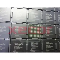
XCV150-5BG256I FPGA - Field Programmable Gate Array
Inventory:5,914
- 90-day after-sales guarantee
- 365 Days Quality Guarantee
- Genuine Product Guarantee
- 7*24 hours service quarantee
-
Part Number : XCV150-5BG256I
-
Package/Case : BGA-256
-
Brands : Xilinx
-
Components Categories : FPGAs
-
Datesheet : XCV150-5BG256I DataSheet (PDF)
The XCV150-5BG256I is a Field-Programmable Gate Array (FPGA) featuring 1.5 million system gates, 18,432 logic cells, and 360 I/O pins. It operates at a speed grade of -5 and is ideal for high-performance digital logic applications requiring complex programmable logic functionality. (Note: The pin configuration below is a general representation. Refer to the specific datasheet for precise details.) Include a circuit diagram illustrating the connections and operation of the XCV150-5BG256I FPGA for a visual representation. Note: For detailed technical specifications, please refer to the XCV150-5BG256I datasheet. Functionality The XCV150-5BG256I FPGA offers extensive programmable logic resources to design and implement sophisticated digital systems with high levels of customization and performance. Usage Guide Q: Can the XCV150-5BG256I be cascaded with other FPGAs for increased functionality? Q: Does the XCV150-5BG256I support partial reconfiguration of logic cells? For comparable FPGA solutions, consider these alternatives to the XCV150-5BG256I:Overview of XCV150-5BG256I
Pinout
Circuit Diagram
Key Features
Application
Frequently Asked Questions
A: Yes, multiple XCV150-5BG256I FPGAs can be cascaded together to increase the overall logic capacity and functionality of the system.
A: Yes, the XCV150-5BG256I allows for partial reconfiguration of specific logic cells, providing flexibility in dynamic system updates.Equivalent
Specifications
The followings are basic parameters of the part selected concerning the characteristics of the part and categories it belongs to.
| Product Category | FPGA - Field Programmable Gate Array | Series | XCV150 |
| Number of Logic Elements | 3888 LE | Adaptive Logic Modules - ALMs | 1728 ALM |
| Embedded Memory | 48 kbit | Number of I/Os | 180 I/O |
| Supply Voltage - Min | 2.5 V | Supply Voltage - Max | 2.5 V |
| Minimum Operating Temperature | - 40 C | Maximum Operating Temperature | + 100 C |
| Mounting Style | SMD/SMT | Package / Case | BGA-256 |
| Brand | Xilinx | Embedded Block RAM - EBR | 49152 bit |
| Maximum Operating Frequency | 200 MHz | Number of Gates | 164674 |
| Number of Logic Array Blocks - LABs | 864 LAB | Operating Supply Voltage | 2.5 V |
| Product Type | FPGA - Field Programmable Gate Array | Subcategory | Programmable Logic ICs |
| Tradename | Virtex |
Warranty & Returns
Warranty, Returns, and Additional Information
-
QA & Return Policy
Parts Quality Guarantee: 365 days
Returns for refund: within 90 days
Returns for Exchange: within 90 days
-
Shipping and Package
Shipping:For example, FedEx, SF, UPS, or DHL.UPS, or DHL.
Parts Packaging Guarantee: Featuring 100% ESD anti-static protection, our packaging incorporates high toughness and superior buffering capabilities.
-
Payment
For example, channels like VISA, MasterCard, UnionPay, Western Union, PayPal, and more.
If you have specific payment channel preferences or requirements, please get in touch with our sales team for assistance.
Similar Product

XC68HC711E9CFS2
8-bit Microcontrollers - MCU

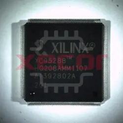
XC95216-15PQG160C
CPLD - Complex Programmable Logic Devices
CY7C64713-128AXC
TQFP-128 packaging

XC2C512-10PQG208C
0.18um Technology 10PQG208C
XC6SLX9-3FTG256C
Small and versatile FPGA
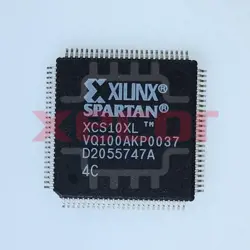
XCS10XL-4VQ100C
96-Cell, CMOS, PBGA144

XC9536-15PC44I
5ns plastic LCC-44
XC95288-15HQ208C
Programmable logic device with 48 macrocells