
XC6SLX75T-3FGG676C
Field Programmable Gate Array, 5831 CLBs, 862MHz, 74637-Cell, CMOS, PBGA676
Inventory:6,079
- 90-day after-sales guarantee
- 365 Days Quality Guarantee
- Genuine Product Guarantee
- 7*24 hours service quarantee
-
Part Number : XC6SLX75T-3FGG676C
-
Package/Case : FBGA-676
-
Brands : Xilinx
-
Components Categories : FPGAs (Field Programmable Gate Array)
-
Datesheet : XC6SLX75T-3FGG676C DataSheet (PDF)
Overview of XC6SLX75T-3FGG676C
FPGA, SPARTAN-6, 348 I/O, FPBGA-676; No. of Logic Blocks:11662; No. of Macrocells:74637Macrocells; FPGA Family:Spartan-6; Logic Case Style:FBGA; No. of Pins:676Pins; No. of Speed Grades:3; Total RAM Bits:3096Kbit; MSL:- RoHS Compliant: Yes
Specifications
The followings are basic parameters of the part selected concerning the characteristics of the part and categories it belongs to.
| Product Category | FPGA - Field Programmable Gate Array | RoHS | Details |
| Series | XC6SLX75T | Number of Logic Elements | 74637 LE |
| Adaptive Logic Modules - ALMs | 11662 ALM | Embedded Memory | 3.02 Mbit |
| Number of I/Os | 348 I/O | Supply Voltage - Min | 1.14 V |
| Supply Voltage - Max | 1.26 V | Minimum Operating Temperature | 0 C |
| Maximum Operating Temperature | + 85 C | Data Rate | 3.2 Gb/s |
| Number of Transceivers | 8 Transceiver | Mounting Style | SMD/SMT |
| Package / Case | FBGA-676 | Brand | Xilinx |
| Distributed RAM | 692 kbit | Embedded Block RAM - EBR | 3096 kbit |
| Maximum Operating Frequency | 1.08 GHz | Moisture Sensitive | Yes |
| Number of Logic Array Blocks - LABs | 5831 LAB | Operating Supply Voltage | 1.2 V |
| Product Type | FPGA - Field Programmable Gate Array | Factory Pack Quantity | 1 |
| Subcategory | Programmable Logic ICs | Tradename | Spartan |
| Unit Weight | 2.696900 oz |
Warranty & Returns
Warranty, Returns, and Additional Information
-
QA & Return Policy
Parts Quality Guarantee: 365 days
Returns for refund: within 90 days
Returns for Exchange: within 90 days
-
Shipping and Package
Shipping:For example, FedEx, SF, UPS, or DHL.UPS, or DHL.
Parts Packaging Guarantee: Featuring 100% ESD anti-static protection, our packaging incorporates high toughness and superior buffering capabilities.
-
Payment
For example, channels like VISA, MasterCard, UnionPay, Western Union, PayPal, and more.
If you have specific payment channel preferences or requirements, please get in touch with our sales team for assistance.
Similar Product
CY37128P100-125AXC
CPLD Ultra37000 Family 3.8K Gates 128 Macro Cells 125MHz 5V 100-Pin TQFP
XC6SLX9-2CSG324C
FPGA Spartan-6 LX Family 9152 Cells 45nm (CMOS) Technology 1.2V 324-Pin CS-BGA
XC6VLX130T-2FFG784I
FPGA - Field Programmable Gate Array XC6VLX130T-2FFG784I
XC6VLX240T-1FF1156I
FPGA - Field Programmable Gate Array XC6VLX240T-1FF1156I
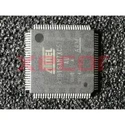
AT91SAM7XC512-AU
ARM Microcontrollers - MCU LQFP IND TEMP
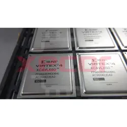
XC4VFX60-11FFG672I
FPGA - Field Programmable Gate Array XC4VFX60-11FFG672I Disconnect standard BOM
XC4VLX60-10FFG668I
FPGA - Field Programmable Gate Array Pb-Free
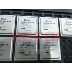
XC4VSX35-10FF668C
FPGA - Field Programmable Gate Array XC4VSX35-10FF668C