
XC2S200E-6FTG256C
357MHz operation speed in 0.15um technology
Inventory:7,158
- 90-day after-sales guarantee
- 365 Days Quality Guarantee
- Genuine Product Guarantee
- 7*24 hours service quarantee
-
Part Number : XC2S200E-6FTG256C
-
Package/Case : FBGA-256
-
Brands : XILINX
-
Components Categories : FPGAs
-
Datesheet : XC2S200E-6FTG256C DataSheet (PDF)
The XC2S200E-6FTG256C is a Spartan-IIE field-programmable gate array (FPGA) from Xilinx. It offers a cost-effective solution for high-density programmable logic applications, featuring a generous number of logic cells and I/O resources. (Note: The pin configuration below is a general representation. Refer to the specific datasheet for precise details.) Include a detailed circuit diagram showcasing the connections and functionality of the XC2S200E-6FTG256C FPGA for a visual representation. Note: For comprehensive technical specifications, please consult the XC2S200E-6FTG256C datasheet. Functionality The XC2S200E-6FTG256C FPGA provides a versatile platform for implementing custom logic functions and signal processing algorithms. It enables users to create complex digital designs and rapidly prototype various applications. Usage Guide Q: Can the XC2S200E-6FTG256C be reprogrammed multiple times? Q: What tools are recommended for programming the XC2S200E-6FTG256C? For similar FPGA solutions, consider these alternatives to the XC2S200E-6FTG256C:Overview of XC2S200E-6FTG256C
Pinout
Circuit Diagram
Key Features
Application
Frequently Asked Questions
A: Yes, the XC2S200E-6FTG256C is a reprogrammable FPGA, allowing users to modify the configuration multiple times as needed for different applications.
A: Xilinx provides software tools such as Vivado Design Suite for programming and configuring the XC2S200E-6FTG256C FPGA.Equivalent
Specifications
The followings are basic parameters of the part selected concerning the characteristics of the part and categories it belongs to.
| Product Category | FPGA - Field Programmable Gate Array | Series | XC2S200E |
| Number of Logic Elements | 5292 LE | Adaptive Logic Modules - ALMs | 2352 ALM |
| Embedded Memory | 56 kbit | Number of I/Os | 182 I/O |
| Supply Voltage - Min | 1.8 V | Supply Voltage - Max | 1.8 V |
| Minimum Operating Temperature | 0 C | Maximum Operating Temperature | + 85 C |
| Mounting Style | SMD/SMT | Package / Case | FBGA-256 |
| Brand | Xilinx | Distributed RAM | 75264 bit |
| Embedded Block RAM - EBR | 56 kbit | Maximum Operating Frequency | 275 MHz |
| Moisture Sensitive | Yes | Number of Logic Array Blocks - LABs | 1176 LAB |
| Operating Supply Voltage | 1.8 V | Product Type | FPGA - Field Programmable Gate Array |
| Subcategory | Programmable Logic ICs | Tradename | Spartan |
Warranty & Returns
Warranty, Returns, and Additional Information
-
QA & Return Policy
Parts Quality Guarantee: 365 days
Returns for refund: within 90 days
Returns for Exchange: within 90 days
-
Shipping and Package
Shipping:For example, FedEx, SF, UPS, or DHL.UPS, or DHL.
Parts Packaging Guarantee: Featuring 100% ESD anti-static protection, our packaging incorporates high toughness and superior buffering capabilities.
-
Payment
For example, channels like VISA, MasterCard, UnionPay, Western Union, PayPal, and more.
If you have specific payment channel preferences or requirements, please get in touch with our sales team for assistance.
Similar Product

XC95144XL-10TQG144I
XC95144XL-10TQG144I XC95144XL-10TQG144I, CPLD XC9500XL Flash 144 Cells, 117 I/O, 8 Labs, ISP, 3 → 3.6 V 144-Pin TQFP
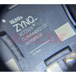
XC7Z020-1CLG484C
Multi-purpose peripheral, Cutting-edge CMOS technology, Quad Flat No-Lead package, Suitable for various applications
XC7S50-1CSGA324I
1098MHz clock frequency
XC6SLX9-3TQG144I
XC6SLX9-3TQG144I is a field-programmable gate array (FPGA) from the Spartan-6 LX family, featuring 9152 cells and built using 45nm CMOS technology
XC6SLX45-3CSG324I
XC6SLX45-3CSG324I is a RoHS compliant product
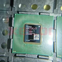
XC7A200T-2FBG676I
Versatile device for a range of applications
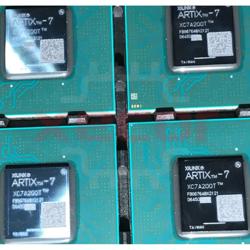
XC7A200T-2FBG676C
Commercial Grade RoHS compliant for environmentally-friendly operation
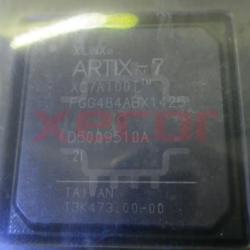
XC7A100T-2FGG484I
XILINX - XC7A100T-2FGG484I - FPGA, ARTIX-7, 285 I/O, FPBGA-484