
LFXP3C-3TN144C
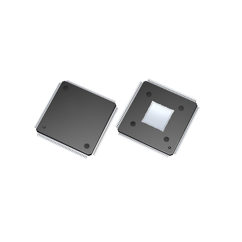
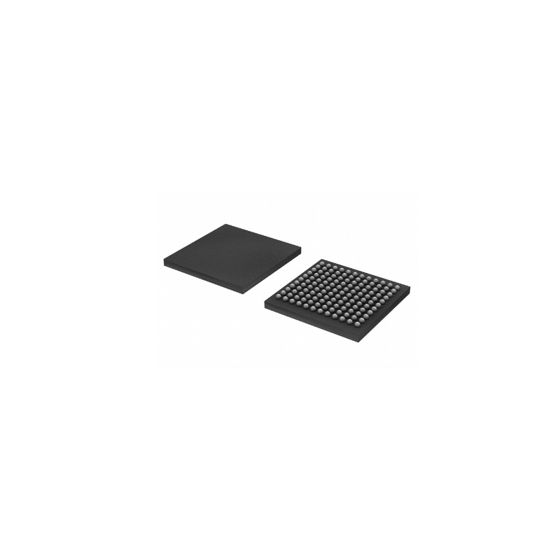
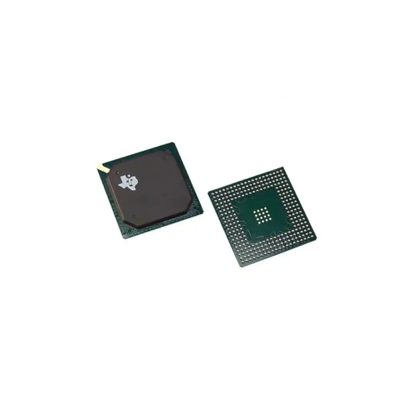
LFXP3C-3TN144C 144-LQFP Field Programmable Gate Array
Inventory:7,781
- 90-day after-sales guarantee
- 365 Days Quality Guarantee
- Genuine Product Guarantee
- 7*24 hours service quarantee
-
Part Number : LFXP3C-3TN144C
-
Package/Case : 144-LQFP
-
Brands : Lattice Semiconductor Corporation
-
Components Categories : FPGAs
-
Datesheet : LFXP3C-3TN144C DataSheet (PDF)
The LFXP3C-3TN144C is a low-cost, low-power FPGA (Field-Programmable Gate Array) featuring an abundant supply of logic elements and general-purpose I/Os. With its compact size and efficient design, this FPGA is ideal for various applications requiring programmable logic. (Note: The pinout information provided below serves as a general representation. Refer to the specific datasheet for precise details.) Include a circuit diagram illustrating the connections and operation of the LFXP3C-3TN144C FPGA for a clearer understanding of its functionality. Note: For detailed technical specifications, please refer to the LFXP3C-3TN144C datasheet. Functionality The LFXP3C-3TN144C FPGA provides a reprogrammable platform for implementing digital logic functions, offering flexibility and customization for various applications. Usage Guide Q: Can the LFXP3C-3TN144C be used for real-time applications? Q: Is the LFXP3C-3TN144C suitable for low-power IoT devices? For alternatives with similar functionalities, consider the following products:Overview of LFXP3C-3TN144C
Pinout
Circuit Diagram
Key Features
Application
Frequently Asked Questions
A: While the LFXP3C-3TN144C is capable of fast operation, its suitability for real-time applications depends on the specific requirements of the application.
A: Yes, the low-power characteristics of the LFXP3C-3TN144C make it a good choice for IoT devices requiring programmable logic functionality.Equivalent
Specifications
The followings are basic parameters of the part selected concerning the characteristics of the part and categories it belongs to.
| Series | XP | Package | Tray |
| Product Status | Obsolete | Programmabe | Not Verified |
| Number of Logic Elements/Cells | 3000 | Total RAM Bits | 55296 |
| Number of I/O | 100 | Voltage - Supply | 1.71V ~ 3.465V |
| Mounting Type | Surface Mount | Operating Temperature | 0°C ~ 85°C (TJ) |
| Package / Case | 144-LQFP | Supplier Device Package | 144-TQFP (20x20) |
| Base Product Number | LFXP3 |
Warranty & Returns
Warranty, Returns, and Additional Information
-
QA & Return Policy
Parts Quality Guarantee: 365 days
Returns for refund: within 90 days
Returns for Exchange: within 90 days
-
Shipping and Package
Shipping:For example, FedEx, SF, UPS, or DHL.UPS, or DHL.
Parts Packaging Guarantee: Featuring 100% ESD anti-static protection, our packaging incorporates high toughness and superior buffering capabilities.
-
Payment
For example, channels like VISA, MasterCard, UnionPay, Western Union, PayPal, and more.
If you have specific payment channel preferences or requirements, please get in touch with our sales team for assistance.
Similar Product

LFXP2-17E-5FTN256C
35MHz frequency, 17000 cells, CMOS technology, PBGA256 package, 17 X 17 MM size, lead-free, FTBGA-256
LFEC10E-4FN484C
This cutting-edge IC FPGA boasts advanced routing capabilities
LFEC3E-4TN144C
Field Programmable Gate Array with 3.1K LUTs, Lead-Free
LFE3-17EA-6MG328C
This CPLD/FPGA has a 10x10 configuration with 2125 effective gates for versatile programmable functionality
LFE3-17EA-8FTN256C
FPGA featuring 17.3K LUTs and -8 speed
LFXP6C-5TN144C
23552bit, 6000 Blocks
LFE3-35EA-8FN484C
65nm Technology FPGA with 33000 Cells
LFE2-12E-5FN256C
24576bit, 12000 Blocks