
EP4CE40F23C6N
FPGA Cyclone® IV E Family 39600 Cells 60nm Technology 1.2V 484-Pin FBGA
Inventory:6,570
- 90-day after-sales guarantee
- 365 Days Quality Guarantee
- Genuine Product Guarantee
- 7*24 hours service quarantee
-
Part Number : EP4CE40F23C6N
-
Package/Case : FBGA-484
-
Brands : Intel
-
Components Categories : FPGAs
-
Datesheet : EP4CE40F23C6N DataSheet (PDF)
The EP4CE40F23C6N is a FPGA (Field-Programmable Gate Array) device featuring 39,600 logic elements, 1,272 Kbits of embedded memory, and 522 user I/Os. It is designed for high-performance and low-power applications, offering flexibility and reconfigurability in digital designs. (Note: The pin configuration below is a general representation. Refer to the specific datasheet for precise details.) Include a circuit diagram illustrating the connections and operation of the EP4CE40F23C6N FPGA for a visual representation. Note: For detailed technical specifications, please refer to the EP4CE40F23C6N datasheet. Functionality The EP4CE40F23C6N FPGA offers a programmable platform for implementing complex digital functions, enabling customization and versatility in various applications. Usage Guide Q: Can the EP4CE40F23C6N be used for real-time applications? Q: What programming languages are commonly used to program the EP4CE40F23C6N? For similar functionalities, consider these alternatives to the EP4CE40F23C6N:Overview of EP4CE40F23C6N
Pinout
Circuit Diagram
Key Features
Application
Frequently Asked Questions
A: Yes, the EP4CE40F23C6N FPGA is capable of handling real-time processing tasks due to its high logic density and configurable nature.
A: Verilog and VHDL are the most commonly used hardware description languages for programming FPGAs like the EP4CE40F23C6N.Equivalent
Specifications
The followings are basic parameters of the part selected concerning the characteristics of the part and categories it belongs to.
| Product Category | FPGA - Field Programmable Gate Array | Shipping Restrictions | This product may require additional documentation to export from the United States. |
| RoHS | Details | Series | EP4CE40 Cyclone IV E |
| Number of Logic Elements | 39600 LE | Embedded Memory | 1134 kbit |
| Number of I/Os | 328 I/O | Supply Voltage - Min | 1.15 V |
| Supply Voltage - Max | 1.25 V | Minimum Operating Temperature | 0 C |
| Maximum Operating Temperature | + 70 C | Mounting Style | SMD/SMT |
| Package / Case | FBGA-484 | Brand | Altera |
| Maximum Operating Frequency | 200 MHz | Moisture Sensitive | Yes |
| Number of Logic Array Blocks - LABs | 2475 LAB | Operating Supply Voltage | 1.2 V |
| Product Type | FPGA - Field Programmable Gate Array | Factory Pack Quantity | 60 |
| Subcategory | Programmable Logic ICs | Total Memory | 1134 kbit |
| Tradename | Cyclone IV | Part # Aliases | 971897 |
| Unit Weight | 0.077955 oz |
Warranty & Returns
Warranty, Returns, and Additional Information
-
QA & Return Policy
Parts Quality Guarantee: 365 days
Returns for refund: within 90 days
Returns for Exchange: within 90 days
-
Shipping and Package
Shipping:For example, FedEx, SF, UPS, or DHL.UPS, or DHL.
Parts Packaging Guarantee: Featuring 100% ESD anti-static protection, our packaging incorporates high toughness and superior buffering capabilities.
-
Payment
For example, channels like VISA, MasterCard, UnionPay, Western Union, PayPal, and more.
If you have specific payment channel preferences or requirements, please get in touch with our sales team for assistance.
Similar Product

EP1K100QC208-1N
FPGA ACEX 1K Family 100K Gates 4992 Cells 333.33MHz 0.22um Technology 2.5V 208-Pin PQFP
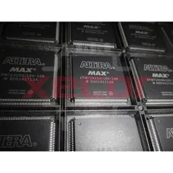
EPM7192SQI160-10N
This device is supplied in a tray packaging to ensure safe handling during transportation and storage
EPM7128AETI100-7N
Programmable Logic Device for Various Applications
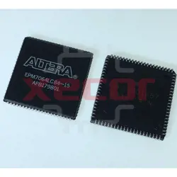
EPM7064LC84-15
Operating frequency of 76.9MHz at 5V
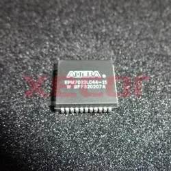
EPM7032LC44-15
High-performance programmable logic device

EPM7032LC44-12
12 Nanosecond Propagation Delay for Quick Data Processing

EPM7032LC44-10
EPM7032LC44-10 is a complex EEPLD with 32 cells and a 10ns propagation delay, housed in a 44-pin plastic PLCC package

EPM3512AQI208-10N
High density integrated circuit