
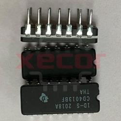
CD4013BF3A
IC CERDIL14 CD4013BF3A Dual D-Type Flip Flop
Inventory:3,796
- 90-day after-sales guarantee
- 365 Days Quality Guarantee
- Genuine Product Guarantee
- 7*24 hours service quarantee
-
Part Number : CD4013BF3A
-
Package/Case : CDIP (J)-14
-
Brands : TI
-
Components Categories : Flip Flops
-
Datesheet : CD4013BF3A DataSheet (PDF)
Overview of CD4013BF3A
The CD4013BF3A is a dual D-type flip-flop integrated circuit (IC) in a 14-pin package. It features independent data inputs (D0 and D1) and complementary outputs (Q and Q̅) for each flip-flop. The clock input (CP) controls the state of the flip-flops, with data being transferred on the rising edge of the clock signal.This IC operates with a wide voltage range, typically between 3V and 18V, making it suitable for a variety of electronic applications. It has a high-speed operation with a maximum propagation delay of 250 ns, allowing for quick data processing.The CD4013BF3A is commonly used in digital circuits for storing and transferring data in sequential logic applications. It is known for its reliability and robustness, making it a popular choice among electronics enthusiasts and professionals.
Key Features
Application
Specifications
The followings are basic parameters of the part selected concerning the characteristics of the part and categories it belongs to.
| Number of channels | 2 | Technology family | CD4000 |
| Supply voltage (min) (V) | 3 | Supply voltage (max) (V) | 18 |
| Input type | Standard CMOS | Output type | Push-Pull |
| Clock frequency (max) (MHz) | 24 | IOL (max) (mA) | 6.8 |
| IOH (max) (mA) | -6.8 | Supply current (max) (µA) | 600 |
| Features | Balanced outputs, Positive input clamp diode, Standard speed (tpd > 50ns) | Operating temperature range (°C) | -55 to 125 |
| Rating | Military |
Warranty & Returns
Warranty, Returns, and Additional Information
-
QA & Return Policy
Parts Quality Guarantee: 365 days
Returns for refund: within 90 days
Returns for Exchange: within 90 days
-
Shipping and Package
Shipping:For example, FedEx, SF, UPS, or DHL.UPS, or DHL.
Parts Packaging Guarantee: Featuring 100% ESD anti-static protection, our packaging incorporates high toughness and superior buffering capabilities.
-
Payment
For example, channels like VISA, MasterCard, UnionPay, Western Union, PayPal, and more.
If you have specific payment channel preferences or requirements, please get in touch with our sales team for assistance.
Similar Product
CD4013BF
The CD4013BF is a dual D flip-flop integrated circuit
CD4094BE
8-18V Voltage Range
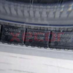
CD40107BE
Low power consumption at 4uA
CD4017BEE4
Integrated circuit for counting
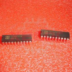
CD74HC573E
High Speed CMOS Logic Octal Transparent Latches with 3-State Outputs
CD40107BM
Logic Gates CMOS Dual 2-Input NAND Buffer/Driver
CD4050BDR
6-ch, 3-V to 18-V buffers
CD4093BPWR
NAND Gate 4-Element 2-IN CMOS 14-Pin TSSOP T/R