
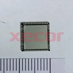
A3P1000-FGG484
With its versatile architecture, this FPGA is ideal for a wide range of applications
Inventory:7,810
- 90-day after-sales guarantee
- 365 Days Quality Guarantee
- Genuine Product Guarantee
- 7*24 hours service quarantee
-
Part Number : A3P1000-FGG484
-
Package/Case : BGA
-
Brands : Microchip Technology
-
Components Categories : FPGAs
-
Datesheet : A3P1000-FGG484 DataSheet (PDF)
The A3P1000-FGG484 is a field-programmable gate array (FPGA) featuring a high logic density and extensive
reconfigurability. With 1,000,000 system gates, it offers a versatile platform for digital circuit
implementation and prototyping. The FPGA supports reprogramming of its configuration to adapt to different
application requirements, making it a valuable component for design flexibility.
(Note: The pin configuration below is a general representation. Refer to the specific datasheet for precise
details.) Include a circuit diagram illustrating the connections and operation of the A3P1000-FGG484 FPGA for a visual
representation. Note: For detailed technical specifications, please refer to the A3P1000-FGG484 datasheet. Functionality The A3P1000-FGG484 is a highly reconfigurable field-programmable gate array designed to accommodate
sophisticated digital designs and flexible system implementations. It offers extensive logic resources and
customizable functionality to meet diverse application requirements. Usage Guide Q: Can the A3P1000-FGG484 support real-time signal processing applications? Q: Is the A3P1000-FGG484 suitable for low-power embedded systems? For similar functionalities, consider these alternatives to the A3P1000-FGG484:Overview of A3P1000-FGG484
Pinout
Circuit Diagram
Key Features
Application
Frequently Asked Questions
A: Yes, the
A3P1000-FGG484 FPGA is capable of efficient real-time signal processing and can be tailored to specific signal
processing requirements.
A: Despite its high logic
density, the A3P1000-FGG484 is designed for efficient power utilization, making it suitable for integration
into low-power embedded systems.Equivalent
Specifications
The followings are basic parameters of the part selected concerning the characteristics of the part and categories it belongs to.
| Product Type | ProASIC3 | eNVM | No |
| eSRAM | No | Logic Elements | 11K |
| Fabric RAM | 144 Kbits | Fabric ROM | 1 Kbits |
| Fabric uPROM | No | Math Blocks 18x18 | No |
| PCIe | No | MSS I/O | No |
| FPGA I/O | No | Max User I/O | 300 |
| Data Security | No | Analog | No |
| Temp min | -55C | Temp max | 135C |
Warranty & Returns
Warranty, Returns, and Additional Information
-
QA & Return Policy
Parts Quality Guarantee: 365 days
Returns for refund: within 90 days
Returns for Exchange: within 90 days
-
Shipping and Package
Shipping:For example, FedEx, SF, UPS, or DHL.UPS, or DHL.
Parts Packaging Guarantee: Featuring 100% ESD anti-static protection, our packaging incorporates high toughness and superior buffering capabilities.
-
Payment
For example, channels like VISA, MasterCard, UnionPay, Western Union, PayPal, and more.
If you have specific payment channel preferences or requirements, please get in touch with our sales team for assistance.
Similar Product
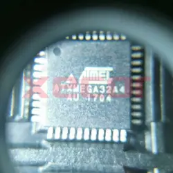
ATXMEGA32A4-AU
Microcontroller ATXMEGA32A4-AU provides a balance of performance and memory capacity with 32kb of Flash memory

XC7A35T-1FGG484C
Artix 7 FPGA, BGA-484

XC7A35T-1FGG484I
XILINX - XC7A35T-1FGG484I - FPGA, ARTIX-7, 250 I/O, FPBGA-484

ATMEGA32U4-MUR
8-bit Microcontrollers - MCU USB 32K FLASH 16 MHz
ATXMEGA256A3U-MH
8-bit microcontroller from the AVR8 family with 256KB of flash memory and 16KB of RAM
OMAPL138BZCEA3
This product is designed with the OMAP-L1x architecture, providing efficient 32-bit processing capabilities for a wide range of applications
OMAPL138BZWTA3
OMAPL138BZWTA3 is a digital signal processor and controller designed for low-power applications

XC7A35T-L1CSG324I
Tin/Silver/Copper (Sn/Ag/Cu) - Durable and reliable materials