
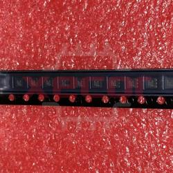
CSD17575Q3
MOSFET 30V, N-channel NexFET Pwr MOSFET
| Quantity | Unit Price(USD) | Ext. Price |
|---|---|---|
| 1 | $0.765 | $0.76 |
| 10 | $0.639 | $6.39 |
| 30 | $0.576 | $17.28 |
| 100 | $0.514 | $51.40 |
| 500 | $0.418 | $209.00 |
| 1000 | $0.398 | $398.00 |
Inventory:7,122
- 90-day after-sales guarantee
- 365 Days Quality Guarantee
- Genuine Product Guarantee
- 7*24 hours service quarantee
-
Part Number : CSD17575Q3
-
Package/Case : 8-VSON-CLIP (3.3x3.3)
-
Brands : TI
-
Components Categories : FETs, MOSFETsSingle FETs, MOSFETs
-
Datesheet : CSD17575Q3 DataSheet (PDF)
The CSD17575Q3 is a high-frequency, synchronous buck NexFET™ power block designed for portable applications. This power block integrates high-side and low-side MOSFETs to minimize losses and provide efficient power conversion. (Note: The pin configuration below is a general representation. Refer to the specific datasheet for precise details.) Incorporate a circuit diagram illustrating the connections and operation of the CSD17575Q3 for a visual representation. Note: For detailed technical specifications, please refer to the CSD17575Q3 datasheet. Functionality The CSD17575Q3 is a high-frequency, synchronous buck power block designed for efficient power conversion in portable applications. It integrates high-side and low-side MOSFETs for minimized losses and compact designs. Usage Guide Q: What is the maximum input voltage for the CSD17575Q3? Q: Is the CSD17575Q3 suitable for low-power applications? For similar functionalities, consider these alternatives to the CSD17575Q3:Overview of CSD17575Q3
Pinout
Circuit Diagram
Key Features
Application
Frequently Asked Questions
A: The CSD17575Q3 can handle a maximum input voltage as specified in the datasheet.
A: Yes, the CSD17575Q3 is designed for efficient power conversion, making it suitable for low-power and battery-powered applications.Equivalent
Specifications
The followings are basic parameters of the part selected concerning the characteristics of the part and categories it belongs to.
| Source Content uid | CSD17575Q3 | Pbfree Code | Yes |
| Rohs Code | No | Part Life Cycle Code | Active |
| Ihs Manufacturer | TEXAS INSTRUMENTS INC | Package Description | SMALL OUTLINE, S-PDSO-N5 |
| Reach Compliance Code | not_compliant | ECCN Code | EAR99 |
| HTS Code | 8541.29.00.95 | Samacsys Manufacturer | Texas Instruments |
| Additional Feature | AVALANCHE RATED | Avalanche Energy Rating (Eas) | 115 mJ |
| Case Connection | DRAIN | Configuration | SINGLE WITH BUILT-IN DIODE |
| DS Breakdown Voltage-Min | 30 V | Drain Current-Max (ID) | 27 A |
| Drain-source On Resistance-Max | 0.0032 Ω | FET Technology | METAL-OXIDE SEMICONDUCTOR |
| Feedback Cap-Max (Crss) | 204 pF | JESD-30 Code | R-PDSO-N8 |
| JESD-609 Code | e3 | Moisture Sensitivity Level | 1 |
| Number of Elements | 1 | Number of Terminals | 8 |
| Operating Mode | ENHANCEMENT MODE | Operating Temperature-Max | 150 °C |
| Operating Temperature-Min | -55 °C | Package Body Material | PLASTIC/EPOXY |
| Package Shape | RECTANGULAR | Package Style | SMALL OUTLINE |
| Peak Reflow Temperature (Cel) | 260 | Polarity/Channel Type | N-CHANNEL |
| Pulsed Drain Current-Max (IDM) | 240 A | Surface Mount | YES |
| Terminal Finish | MATTE TIN | Terminal Form | NO LEAD |
| Terminal Position | DUAL | Time@Peak Reflow Temperature-Max (s) | 30 |
| Transistor Application | SWITCHING | Transistor Element Material | SILICON |
Warranty & Returns
Warranty, Returns, and Additional Information
-
QA & Return Policy
Parts Quality Guarantee: 365 days
Returns for refund: within 90 days
Returns for Exchange: within 90 days
-
Shipping and Package
Shipping:For example, FedEx, SF, UPS, or DHL.UPS, or DHL.
Parts Packaging Guarantee: Featuring 100% ESD anti-static protection, our packaging incorporates high toughness and superior buffering capabilities.
-
Payment
For example, channels like VISA, MasterCard, UnionPay, Western Union, PayPal, and more.
If you have specific payment channel preferences or requirements, please get in touch with our sales team for assistance.
Similar Product
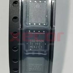
CSD18504Q5A
The CSD18504Q5A MOSFET is designed for efficient power management applications, offering high performance and reliability in a compact form factor
CSD18503Q5A
Texas Instruments CSD18503Q5A N-channel MOSFET Transistor, 145 A, 40 V, 8-Pin SON
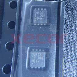
CSD25402Q3A
MOSFET P-CH Pwr MOSFET
CSD19536KTT
CSD19536KTT is a power MOSFET from NexFET™, with N-channel configuration suitable for various applications
CSD19538Q2
Trans MOSFET N-CH Si 100V 14.4A 6-Pin WSON EP T/R
CSD18543Q3A
The specifications of product CSD18543Q3A include a 60-volt N-channel NexFET™ power MOSFET
CSD19532Q5B
MOSFET 100V 4.0 mOhm N-Ch NexFET Power MOSFET
CSD19531Q5A
Trans MOSFET N-CH Si 100V 100A 8-Pin VSONP EP T/R