
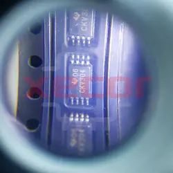
CDCLVP1204RGTR
Clock Fanout Buffer 4-OUT 2-IN 1:4 16-Pin VQFN EP T/R
| Quantity | Unit Price(USD) | Ext. Price |
|---|---|---|
| 1 | $2.238 | $2.24 |
| 10 | $1.916 | $19.16 |
| 30 | $1.712 | $51.36 |
| 100 | $1.505 | $150.50 |
| 500 | $1.411 | $705.50 |
| 1000 | $1.370 | $1,370.00 |
Inventory:4,855
- 90-day after-sales guarantee
- 365 Days Quality Guarantee
- Genuine Product Guarantee
- 7*24 hours service quarantee
-
Part Number : CDCLVP1204RGTR
-
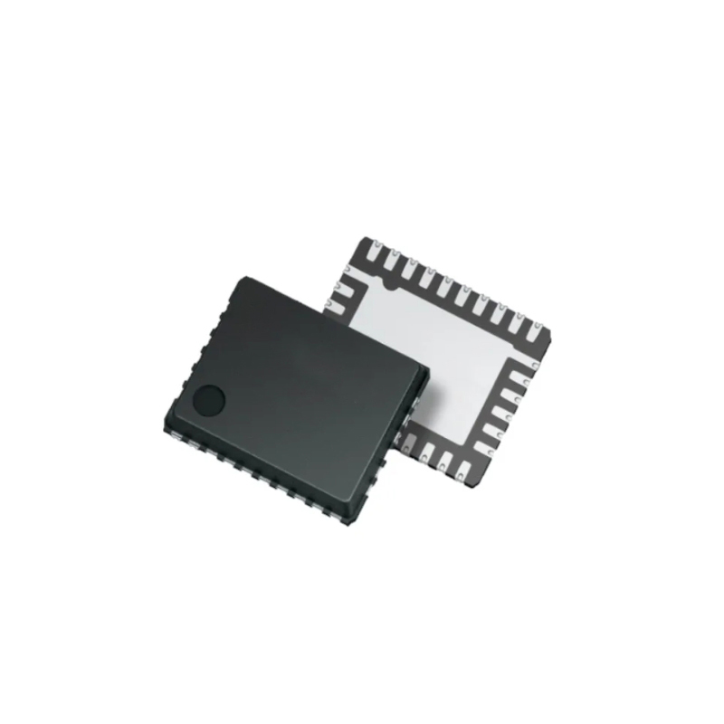
Package/Case : VQFN-16
-
Brands : TI
-
Components Categories : Clock Buffers, Drivers
-
Datesheet : CDCLVP1204RGTR DataSheet (PDF)
Overview of CDCLVP1204RGTR
The CDCLVP1204 is a highly versatile, low additive jitter buffer that can generate four copies of LVPECL clock outputs from one of two selectable LVPECL, LVDS, or LVCMOS inputs for a variety of communication applications. It has a maximum clock frequency up to 2 GHz. The CDCLVP1204 features an on-chip multiplexer (MUX) for selecting one of two inputs that can be easily configured solely through a control terminal. The overall additive jitter performance is less than 0.1 ps, RMS from 10 kHz to 20 MHz, and overall output skew is as low as 15 ps, making the device a perfect choice for use in demanding applications.
The CDCLVP1204 clock buffer distributes one of two selectable clock inputs (IN0, IN1) to four pairs of differential LVPECL clock outputs (OUT0, OUT3) with minimum skew for clock distribution. The CDCLVP1204 can accept two clock sources into an input multiplexer. The inputs can be LVPECL, LVDS, or LVCMOS/LVTTL.
The CDCLVP1204 is specifically designed for driving 50-Ω transmission lines. When driving the inputs in single-ended mode, the LVPECL bias voltage (VAC_REF) must be applied to the unused negative input terminal. However, for high-speed performance up to 2 GHz, differential mode is strongly recommended.
The CDCLVP1204 is characterized for operation from –40°C to +85°C.
Key Features
- 2:4 Differential Buffer
- Selectable Clock Inputs Through Control Terminal
- Universal Inputs Accept LVPECL, LVDS, and
LVCMOS/LVTTL - Four LVPECL Outputs
- Maximum Clock Frequency: 2 GHz
- Maximum Core Current Consumption: 45 mA
- Very Low Additive Jitter: <100 fs, RMS in 10-kHz
to 20-MHz Offset Range:- 57 fs, RMS (typical) at 122.88 MHz
- 48 fs, RMS (typical) at 156.25 MHz
- 30 fs, RMS (typical) at 312.5 MHz
- 2.375-V to 3.6-V Device Power Supply
- Maximum Propagation Delay: 450 ps
- Maximum Output Skew: 15 ps
- LVPECL Reference Voltage, VAC_REF, Available
for Capacitive-Coupled Inputs - Industrial Temperature Range: –40°C to +85°C
- Supports 105°C PCB Temperature (Measured at
Thermal Pad) - ESD Protection Exceeds 2 kV (HBM)
Specifications
The followings are basic parameters of the part selected concerning the characteristics of the part and categories it belongs to.
| Function | Differential | Additive RMS jitter (typ) (fs) | 57 |
| Output frequency (max) (MHz) | 2000 | Number of outputs | 4 |
| Output supply voltage (V) | 2.5, 3.3 | Core supply voltage (V) | 2.5, 3.3 |
| Output skew (ps) | 15 | Features | 2:4 fanout |
| Operating temperature range (°C) | -40 to 85 | Rating | Catalog |
| Output type | LVPECL | Input type | LVCMOS, LVDS, LVPECL |
Warranty & Returns
Warranty, Returns, and Additional Information
-
QA & Return Policy
Parts Quality Guarantee: 365 days
Returns for refund: within 90 days
Returns for Exchange: within 90 days
-
Shipping and Package
Shipping:For example, FedEx, SF, UPS, or DHL.UPS, or DHL.
Parts Packaging Guarantee: Featuring 100% ESD anti-static protection, our packaging incorporates high toughness and superior buffering capabilities.
-
Payment
For example, channels like VISA, MasterCard, UnionPay, Western Union, PayPal, and more.
If you have specific payment channel preferences or requirements, please get in touch with our sales team for assistance.
Similar Product
CDCV304PW
The CDCV304PW is a high-performance clock buffer and frequency divider chip designed for use in telecommunications and networking systems
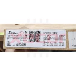
CDCLVC1104PWR
8-pin TSSOP package
CDCI6214RGER
Clock Generators & Support Products PCIe Gen4 support ultra-low power clock generator with four programmable outputs & EEPROM 24-VQFN -40 to 85
CDCLVC1102PWR
Clock Fanout Buffer 2-OUT 1-IN 1:2 8-Pin TSSOP T/R
CDCV304PWR
Versatile clock buffering solution for multiple devices
CDCE62002RHBT
The CDCE62002RHBT is a QFN-32-(5x5) clock generator, frequency synthesizer, and PLL that is ROHS compliant
TLC555CD
Standard Timer Single 0°C 70°C 8-Pin SOIC Tube
CDCE706PWR
Clock Generator 1MHz to 200MHz-IN 300MHz-OUT 20-Pin TSSOP T/R