
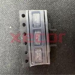
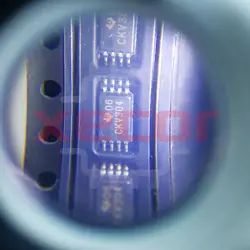
CDCI6214RGER
Clock Generators & Support Products PCIe Gen4 support ultra-low power clock generator with four programmable outputs & EEPROM 24-VQFN -40 to 85
| Quantity | Unit Price(USD) | Ext. Price |
|---|---|---|
| 1 | $8.122 | $8.12 |
| 10 | $7.154 | $71.54 |
| 30 | $6.565 | $196.95 |
| 100 | $6.069 | $606.90 |
Inventory:4,285
- 90-day after-sales guarantee
- 365 Days Quality Guarantee
- Genuine Product Guarantee
- 7*24 hours service quarantee
-
Part Number : CDCI6214RGER
-
Package/Case : 24-VQFN (4x4)
-
Brands : TI
-
Components Categories : Clock Generators, PLLs, Frequency Synthesizers
-
Datesheet : CDCI6214RGER DataSheet (PDF)
Overview of CDCI6214RGER
The CDCI6214 device is an ultra-low power clock generator. The device selects between two independent reference inputs to a phase-locked loop and generates up to four different frequencies on configurable differential output channels and also a copy of the reference clock on a LVCMOS output channel.
Each of the four output channels has a configurable integer divider. Together with the output muxes, this allows up to five different frequencies. Clock distribution dividers are reset in a deterministic way for clean clock gating and glitch-less update capability. Flexible power-down options allow to optimize the device for lowest power consumption in active and standby operation. Typically four 156.25-MHz LVDS outputs consume 150 mW at 1.8 V. Typical RMS jitter of 386 fs for 100-MHz HCSL output enhances system margin for PCIe applications.
The CDCI6214 is configured using internal registers that are accessed by an I2C-compatible serial interface and internal EEPROM.
The CDCI6214 enables high-performance clock trees from a single reference at ultra-low power with a small footprint. The factory- and user-programmable EEPROM make the CDCI6214 ideal as easy-to-use, instant-on clocking solution with low power consumption.
Key Features
- One Configurable High Performance, Low-Power PLL With 4 Programmable Outputs
- RMS Jitter Performance
- Supports PCIe Gen1/ Gen2 / Gen3 / Gen4 without SSC
- Typical Power Consumption: 150 mW at 1.8 V(2)
- Universal Clock Input
- Differential AC-Coupled or LVCMOS: 1 MHz to 250 MHz
- Crystal: 8 MHz to 50 MHz
- Flexible Output Frequencies
- 44.1 kHz to 350 MHz
- Glitchless Output Divider Switching
- Four Individually Configurable Outputs
- LVCMOS, LVDS or HCSL
- Differential AC-Coupled With Programmable Swing (LVDS-, CML-, LVPECL-Compatible)
- Fully Integrated PLL, Configurable Loop Bandwidth: 100 kHz to 3 MHz
- Single or Mixed Supply Operation for Level Translation: 1.8 V, 2.5 V and 3.3 V
- Configurable GPIOs
- Status Signals
- Up to 4 Individual Output Enables
- Output Divider Synchronization
- Flexible Configuration Options
- I2C-Compatible Interface: Up to 400 kHz
- Integrated EEPROM With Two Pages and External Select Pin
- Only Supports 100 Ω Systems
- Industrial Temperature Range: –40ºC to 85ºC
- Small Footprint: 24-Pin VQFN (4 mm × 4 mm)
Specifications
The followings are basic parameters of the part selected concerning the characteristics of the part and categories it belongs to.
| Source Content uid | CDCI6214RGER | Pbfree Code | Yes |
| Rohs Code | Yes | Part Life Cycle Code | Active |
| Ihs Manufacturer | TEXAS INSTRUMENTS INC | Package Description | HVQCCN, |
| Reach Compliance Code | compliant | Date Of Intro | 2017-10-03 |
| Samacsys Manufacturer | Texas Instruments | JESD-30 Code | S-XQCC-N24 |
| JESD-609 Code | e4 | Length | 4 mm |
| Moisture Sensitivity Level | 2 | Number of Terminals | 24 |
| Operating Temperature-Max | 85 °C | Operating Temperature-Min | -40 °C |
| Output Clock Frequency-Max | 350 MHz | Package Body Material | UNSPECIFIED |
| Package Code | HVQCCN | Package Shape | SQUARE |
| Package Style | CHIP CARRIER, HEAT SINK/SLUG, VERY THIN PROFILE | Peak Reflow Temperature (Cel) | 260 |
| Primary Clock/Crystal Frequency-Nom | 50 MHz | Seated Height-Max | 1 mm |
| Supply Voltage-Max | 3.465 V | Supply Voltage-Min | 1.71 V |
| Supply Voltage-Nom | 1.8 V | Surface Mount | YES |
| Technology | CMOS | Temperature Grade | INDUSTRIAL |
| Terminal Finish | Nickel/Palladium/Gold (Ni/Pd/Au) | Terminal Form | NO LEAD |
| Terminal Pitch | 0.5 mm | Terminal Position | QUAD |
| Time@Peak Reflow Temperature-Max (s) | 30 | Width | 4 mm |
| uPs/uCs/Peripheral ICs Type | CLOCK GENERATOR, PROCESSOR SPECIFIC |
Warranty & Returns
Warranty, Returns, and Additional Information
-
QA & Return Policy
Parts Quality Guarantee: 365 days
Returns for refund: within 90 days
Returns for Exchange: within 90 days
-
Shipping and Package
Shipping:For example, FedEx, SF, UPS, or DHL.UPS, or DHL.
Parts Packaging Guarantee: Featuring 100% ESD anti-static protection, our packaging incorporates high toughness and superior buffering capabilities.
-
Payment
For example, channels like VISA, MasterCard, UnionPay, Western Union, PayPal, and more.
If you have specific payment channel preferences or requirements, please get in touch with our sales team for assistance.
Similar Product
CDCV304PW
The CDCV304PW is a high-performance clock buffer and frequency divider chip designed for use in telecommunications and networking systems
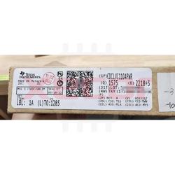
CDCLVC1104PWR
8-pin TSSOP package
CDCLVC1102PWR
Clock Fanout Buffer 2-OUT 1-IN 1:2 8-Pin TSSOP T/R
CDCV304PWR
Versatile clock buffering solution for multiple devices
CDCLVC1103PWR
Clock Fanout Buffer 3-OUT 1-IN 1:3 8-Pin TSSOP T/R
CDCVF2310PW
Clock Buffer CLOCK BUFFER
CDCVF25081PW
Zero Delay Buffer 8-Out Single-Ended 16-Pin TSSOP Tube
CDC2351DB
Clock Driver 10-OUT 1-IN 1:10 24-Pin SSOP Tube