
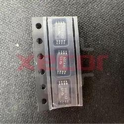
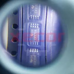
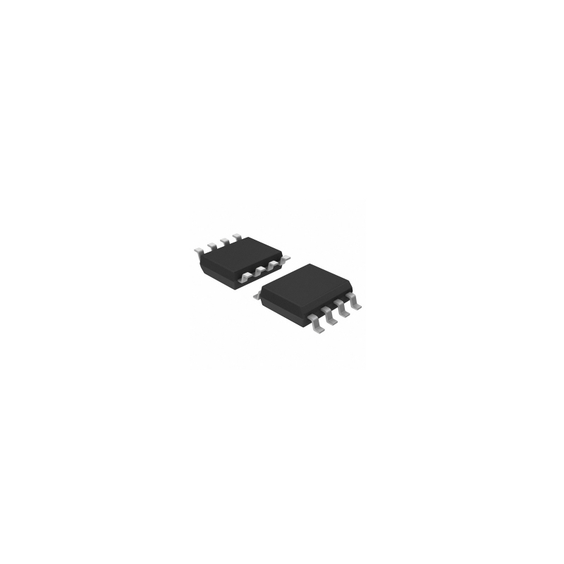
CDCLVC1102PWR
Clock Fanout Buffer 2-OUT 1-IN 1:2 8-Pin TSSOP T/R
| Quantity | Unit Price(USD) | Ext. Price |
|---|---|---|
| 1 | $1.250 | $1.25 |
| 10 | $1.074 | $10.74 |
| 30 | $0.977 | $29.31 |
| 100 | $0.747 | $74.70 |
| 500 | $0.699 | $349.50 |
| 1000 | $0.676 | $676.00 |
Inventory:9,394
- 90-day after-sales guarantee
- 365 Days Quality Guarantee
- Genuine Product Guarantee
- 7*24 hours service quarantee
-
Part Number : CDCLVC1102PWR
-
Package/Case : TSSOP-8
-
Brands : TI
-
Components Categories : Clock buffers
-
Datesheet : CDCLVC1102PWR DataSheet (PDF)
The CDCLVC1102PWR is a low-jitter, high-performance clock buffer designed for clock distribution applications. This IC features low output skew, making it ideal for synchronizing multiple clock signals in various digital systems. (Note: The pin configuration below is a general representation. Refer to the specific datasheet for precise details.) Include a circuit diagram illustrating the connections and operation of the CDCLVC1102PWR IC for a visual representation. Note: For detailed technical specifications, please refer to the CDCLVC1102PWR datasheet. Functionality The CDCLVC1102PWR is a high-performance clock buffer that ensures low jitter and precise clock distribution in digital systems, making it essential for synchronization applications. Usage Guide Q: Can the CDCLVC1102PWR be used for high-speed data applications? Q: Is the CDCLVC1102PWR compatible with 5V systems? For similar functionalities, consider these alternatives to the CDCLVC1102PWR:Overview of CDCLVC1102PWR
Pinout
Circuit Diagram
Key Features
Application
Frequently Asked Questions
A: The CDCLVC1102PWR is designed for clock distribution and synchronization and may not be suitable for high-speed data applications. For high-speed data, consider specialized buffer ICs.
A: The CDCLVC1102PWR operates with a supply voltage range of +2.3V to +3.6V and may not be directly compatible with 5V systems. Ensure proper voltage levels for seamless integration.Equivalent
Specifications
The followings are basic parameters of the part selected concerning the characteristics of the part and categories it belongs to.
| Function | Single-ended | Additive RMS jitter (typ) (fs) | 70 |
| Output frequency (max) (MHz) | 250 | Number of outputs | 2 |
| Output supply voltage (V) | 2.5, 3.3 | Core supply voltage (V) | 2.5, 3.3 |
| Output skew (ps) | 50 | Features | 1:2 fanout, Output enable control |
| Operating temperature range (°C) | -40 to 85 | Rating | Catalog |
| Output type | LVCMOS | Input type | LVCMOS |
Warranty & Returns
Warranty, Returns, and Additional Information
-
QA & Return Policy
Parts Quality Guarantee: 365 days
Returns for refund: within 90 days
Returns for Exchange: within 90 days
-
Shipping and Package
Shipping:For example, FedEx, SF, UPS, or DHL.UPS, or DHL.
Parts Packaging Guarantee: Featuring 100% ESD anti-static protection, our packaging incorporates high toughness and superior buffering capabilities.
-
Payment
For example, channels like VISA, MasterCard, UnionPay, Western Union, PayPal, and more.
If you have specific payment channel preferences or requirements, please get in touch with our sales team for assistance.
Similar Product
CDCV304PW
The CDCV304PW is a high-performance clock buffer and frequency divider chip designed for use in telecommunications and networking systems
CDCLVC1104PWR
8-pin TSSOP package
CDCI6214RGER
Clock Generators & Support Products PCIe Gen4 support ultra-low power clock generator with four programmable outputs & EEPROM 24-VQFN -40 to 85
CDCV304PWR
Versatile clock buffering solution for multiple devices
CDCLVC1103PWR
Clock Fanout Buffer 3-OUT 1-IN 1:3 8-Pin TSSOP T/R
CDCVF2310PW
Clock Buffer CLOCK BUFFER
CDCVF25081PW
Zero Delay Buffer 8-Out Single-Ended 16-Pin TSSOP Tube
CDC2351DB
Clock Driver 10-OUT 1-IN 1:10 24-Pin SSOP Tube