
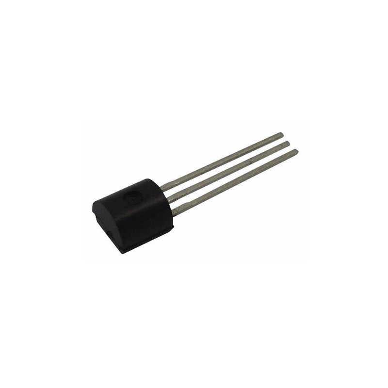
VN2210N2
Trans MOSFET N-CH Si 100V 1.7A 3-Pin TO-39 Bag
| Quantity | Unit Price(USD) | Ext. Price |
|---|---|---|
| 1 | $15.058 | $15.06 |
| 200 | $5.827 | $1,165.40 |
| 500 | $5.623 | $2,811.50 |
| 1000 | $5.521 | $5,521.00 |
Inventory:5,048
- 90-day after-sales guarantee
- 365 Days Quality Guarantee
- Genuine Product Guarantee
- 7*24 hours service quarantee
-
Part Number : VN2210N2
-
Package/Case : TO-39
-
Brands : MICROCHIP
-
Components Categories : FETs, MOSFETsSingle FETs, MOSFETs
-
Datesheet : VN2210N2 DataSheet (PDF)
Overview of VN2210N2
VN2210 is an enhancement-mode (normally-off) transistor that utilizes a vertical DMOS structure and well-proven silicon-gate manufacturing process. This combination produces a device with the power handling capabilities of bipolar transistors, and the high input impedance and positive temperature coefficient inherent in MOS devices. Characteristic of all MOS structures, this device is free from thermal runaway and thermally-induced secondary breakdown. Vertical DMOS FETs are ideally suited to a wide range of switching and amplifying applications where very low threshold voltage, high breakdown voltage, high input impedance, low input capacitance, and fast switching speeds are desired.
Key Features
- Free from secondary breakdown
- Low power drive requirement
- Ease of paralleling
- Low CISS and fast switching speeds
- Excellent thermal stability
- Integral source-drain diode
- High input impedance and high gain
Application
SWITCHINGSpecifications
The followings are basic parameters of the part selected concerning the characteristics of the part and categories it belongs to.
| Source Content uid | VN2210N2 | Rohs Code | Yes |
| Part Life Cycle Code | Active | Ihs Manufacturer | MICROCHIP TECHNOLOGY INC |
| Package Description | TO-39, 3 PIN | Reach Compliance Code | compliant |
| ECCN Code | EAR99 | HTS Code | 8541.29.00.95 |
| Factory Lead Time | 10 Weeks | Samacsys Manufacturer | Microchip |
| Additional Feature | HIGH INPUT IMPEDANCE | Case Connection | DRAIN |
| Configuration | SINGLE WITH BUILT-IN DIODE | DS Breakdown Voltage-Min | 100 V |
| Drain Current-Max (ID) | 1.7 A | Drain-source On Resistance-Max | 0.35 Ω |
| FET Technology | METAL-OXIDE SEMICONDUCTOR | Feedback Cap-Max (Crss) | 65 pF |
| JEDEC-95 Code | TO-39 | JESD-30 Code | O-MBCY-W3 |
| JESD-609 Code | e4 | Number of Elements | 1 |
| Number of Terminals | 3 | Operating Mode | ENHANCEMENT MODE |
| Operating Temperature-Max | 150 °C | Operating Temperature-Min | -55 °C |
| Package Body Material | METAL | Package Shape | ROUND |
| Package Style | CYLINDRICAL | Polarity/Channel Type | N-CHANNEL |
| Power Dissipation-Max (Abs) | 0.36 W | Qualification Status | Not Qualified |
| Surface Mount | NO | Terminal Finish | NICKEL GOLD |
| Terminal Form | WIRE | Terminal Position | BOTTOM |
| Transistor Application | SWITCHING | Transistor Element Material | SILICON |
Warranty & Returns
Warranty, Returns, and Additional Information
-
QA & Return Policy
Parts Quality Guarantee: 365 days
Returns for refund: within 90 days
Returns for Exchange: within 90 days
-
Shipping and Package
Shipping:For example, FedEx, SF, UPS, or DHL.UPS, or DHL.
Parts Packaging Guarantee: Featuring 100% ESD anti-static protection, our packaging incorporates high toughness and superior buffering capabilities.
-
Payment
For example, channels like VISA, MasterCard, UnionPay, Western Union, PayPal, and more.
If you have specific payment channel preferences or requirements, please get in touch with our sales team for assistance.
Similar Product
VN2410L-G
Trans MOSFET N-CH Si 240V 0.19A 3-Pin TO-92 Bag
VN2460N8
MOSFET 600V 20Ohm
VN2460N3-G
Trans MOSFET N-CH Si 600V 0.16A 3-Pin TO-92 Bag
VN10KN3
MOSFET 60V 5Ohm
VN0104N3-G
Trans MOSFET N-CH Si 40V 0.35A 3-Pin TO-92 Bag
VN2406L
MOSFET 240V 6Ohm
VN3205N8
MOSFET 50V 0.3Ohm
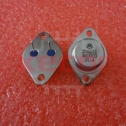
2N6251
Trans GP BJT NPN 275V 10A 3-Pin(2+Tab) TO-3