
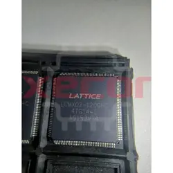
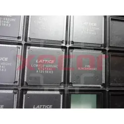
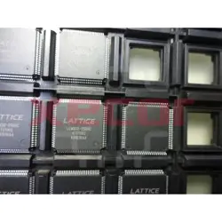
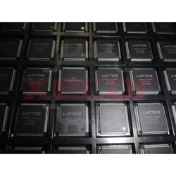
LCMXO256C-3MN100C
CPLD MachXO Family 128 Macro Cells 1.8V/2.5V/3.3V 100-Pin CSBGA
| Quantity | Unit Price(USD) | Ext. Price |
|---|---|---|
| 1 | $8.804 | $8.80 |
| 200 | $3.408 | $681.60 |
| 360 | $3.289 | $1,184.04 |
| 1080 | $3.228 | $3,486.24 |
Inventory:7,860
- 90-day after-sales guarantee
- 365 Days Quality Guarantee
- Genuine Product Guarantee
- 7*24 hours service quarantee
-
Part Number : LCMXO256C-3MN100C
-
Package/Case : BGA
-
Brands : Lattice Semiconductor Corporation
-
Components Categories : FPGAs (Field Programmable Gate Array)
-
Datesheet : LCMXO256C-3MN100C DataSheet (PDF)
Overview of LCMXO256C-3MN100C
MachXO Field Programmable Gate Array (FPGA) IC 78 256 100-LFBGA, CSPBGA
Key Features
- Non-volatile, Infinitely Reconfigurable
- Instant-on – powers up in microseconds
- Single chip, no external configuration memory
- required
- Excellent design security, no bit stream to
- intercept
- Reconfigure SRAM based logic in milliseconds
- SRAM and non-volatile memory programmable
- through JTAG port
- Supports background programming of
- non-volatile memory
- Sleep Mode
- Allows up to 100x static current reduction
- TransFR™ Reconfiguration (TFR)
- In-field logic update while system operates
- High I/O to Logic Density
- 256 to 2280 LUT4s
- 73 to 271 I/Os with extensive package options
- Density migration supported
- Lead free/RoHS compliant packaging
- Embedded and Distributed Memory
- Up to 27.6 Kbits sysMEM™ Embedded Block
- RAM
- Up to 7.5 Kbits distributed RAM
- Dedicated FIFO control logic
- Flexible I/O Buffer
- Programmable sysIO™ buffer supports wide
- range of interfaces:
- − LVCMOS 3.3/2.5/1.8/1.5/1.2
- − LVTTL
- − PCI
- − LVDS, Bus-LVDS, LVPECL, RSDS
- sysCLOCK™ PLLs
- Up to two analog PLLs per device
- Clock multiply, divide, and phase shifting
- System Level Support
- IEEE Standard 1149.1 Boundary Scan
- Onboard oscillator
- Devices operate with 3.3V, 2.5V, 1.8V or 1.2V
- power supply
- IEEE 1532 compliant in-system programming

Specifications
The followings are basic parameters of the part selected concerning the characteristics of the part and categories it belongs to.
| Product Category | FPGA - Field Programmable Gate Array | RoHS | Details |
| Series | LCMXO256C | Number of Logic Elements | 256 LE |
| Adaptive Logic Modules - ALMs | 128 ALM | Embedded Memory | 0 bit |
| Number of I/Os | 78 I/O | Supply Voltage - Min | 1.71 V |
| Supply Voltage - Max | 3.465 V | Minimum Operating Temperature | 0 C |
| Maximum Operating Temperature | + 85 C | Mounting Style | SMD/SMT |
| Package / Case | CSBGA-100 | Brand | Lattice |
| Distributed RAM | 2 kbit | Height | 1.1 mm |
| Length | 8 mm | Maximum Operating Frequency | 500 MHz |
| Moisture Sensitive | Yes | Number of Logic Array Blocks - LABs | 32 LAB |
| Operating Supply Current | 13 mA | Operating Supply Voltage | 1.8 V/2.5 V/3.3 V |
| Product Type | FPGA - Field Programmable Gate Array | Factory Pack Quantity | 360 |
| Subcategory | Programmable Logic ICs | Total Memory | 2 kbit |
| Width | 8 mm | Unit Weight | 0.164694 oz |
Warranty & Returns
Warranty, Returns, and Additional Information
-
QA & Return Policy
Parts Quality Guarantee: 365 days
Returns for refund: within 90 days
Returns for Exchange: within 90 days
-
Shipping and Package
Shipping:For example, FedEx, SF, UPS, or DHL.UPS, or DHL.
Parts Packaging Guarantee: Featuring 100% ESD anti-static protection, our packaging incorporates high toughness and superior buffering capabilities.
-
Payment
For example, channels like VISA, MasterCard, UnionPay, Western Union, PayPal, and more.
If you have specific payment channel preferences or requirements, please get in touch with our sales team for assistance.
Similar Product
LCMXO2-1200HC-4TG144I
FPGA - Field Programmable Gate Array 1280 LUTs 108 I/O 3.3V -4 SPD
LCMXO2-1200HC-4TG144C
FPGA - Field Programmable Gate Array 1280 LUTs 108 I/O 3.3V -4 SPD
LCMXO2-1200HC-4TG100I
FPGA - Field Programmable Gate Array 1280 LUTs 80 I/O 3.3V -4 SPD
LCMXO2-640UHC-4TG144I
CPLD MachXO2 Family 65nm Technology 2.5V/3.3V 144-Pin TQFP Tray
LCMXO640C-3TN144C
CPLD MachXO Family 320 Macro Cells 1.8V/2.5V/3.3V 144-Pin TQFP Tray
LCMXO640C-3FTN256C
CPLD MachXO Family 320 Macro Cells 1.8V/2.5V/3.3V 256-Pin FTBGA Tray
LCMXO2-256HC-4TG100I
CPLD MachXO2 Family 2.5V/3.3V 100-Pin TQFP Tray
LCMXO2-1200HC-4TG100C
FPGA - Field Programmable Gate Array 1280 LUTs 80 I/O 3.3V -4 SPD