
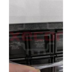
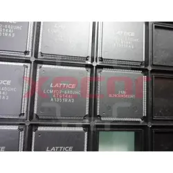
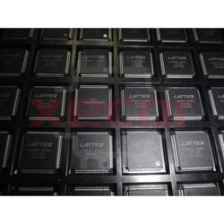
LCMXO2-1200HC-4TG144I
FPGA - Field Programmable Gate Array 1280 LUTs 108 I/O 3.3V -4 SPD
| Quantity | Unit Price(USD) | Ext. Price |
|---|---|---|
| 1 | $7.102 | $7.10 |
| 10 | $6.210 | $62.10 |
| 30 | $5.668 | $170.04 |
| 100 | $5.211 | $521.10 |
Inventory:9,073
- 90-day after-sales guarantee
- 365 Days Quality Guarantee
- Genuine Product Guarantee
- 7*24 hours service quarantee
-
Part Number : LCMXO2-1200HC-4TG144I
-
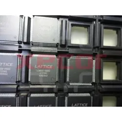
Package/Case : QFP-144
-
Brands : Lattice Semiconductor Corporation
-
Components Categories : FPGAs (Field Programmable Gate Array)
-
Datesheet : LCMXO2-1200HC-4TG144I DataSheet (PDF)
The LCMXO2-1200HC-4TG144I is a low-cost, low-power FPGA (Field-Programmable Gate Array) that offers high-performance and flexibility for various digital logic applications. This FPGA features 1200 LUTs (Look-Up Tables) and is designed to be user-programmable, allowing customization of logic functions. (Note: The pin configuration below is a general representation. Refer to the specific datasheet for precise details.) Include a circuit diagram illustrating the connections and operation of the LCMXO2-1200HC-4TG144I FPGA for visual representation. Note: For detailed technical specifications, please refer to the LCMXO2-1200HC-4TG144I datasheet. Functionality The LCMXO2-1200HC-4TG144I FPGA offers versatile logic implementation capabilities, making it a versatile solution for digital logic applications. It provides users with the flexibility to design and configure custom logic functions based on their requirements. Usage Guide Q: Can the LCMXO2-1200HC-4TG144I be reprogrammed multiple times? Q: Is the LCMXO2-1200HC-4TG144I suitable for high-speed applications? For similar functionalities, consider these alternatives to the LCMXO2-1200HC-4TG144I:Overview of LCMXO2-1200HC-4TG144I
Pinout
Circuit Diagram
Key Features
Application
Frequently Asked Questions
A: Yes, the LCMXO2-1200HC-4TG144I FPGA is designed for multiple reprogramming cycles, allowing users to update and modify their logic designs as needed.
A: While the LCMXO2-1200HC-4TG144I offers high-performance LUTs, for ultra-high-speed applications, consider FPGAs with specialized features for speed optimization.Equivalent
Specifications
The followings are basic parameters of the part selected concerning the characteristics of the part and categories it belongs to.
| Product Category | FPGA - Field Programmable Gate Array | RoHS | Details |
| Series | LCMXO2 | Number of Logic Elements | 1280 LE |
| Adaptive Logic Modules - ALMs | 640 ALM | Embedded Memory | 64 kbit |
| Number of I/Os | 107 I/O | Supply Voltage - Min | 2.375 V |
| Supply Voltage - Max | 3.6 V | Minimum Operating Temperature | - 40 C |
| Maximum Operating Temperature | + 100 C | Mounting Style | SMD/SMT |
| Package / Case | TQFP-144 | Brand | Lattice |
| Distributed RAM | 10 kbit | Embedded Block RAM - EBR | 64 kbit |
| Maximum Operating Frequency | 269 MHz | Moisture Sensitive | Yes |
| Number of Logic Array Blocks - LABs | 160 LAB | Operating Supply Current | 3.49 mA |
| Operating Supply Voltage | 2.5 V/3.3 V | Product Type | FPGA - Field Programmable Gate Array |
| Factory Pack Quantity | 60 | Subcategory | Programmable Logic ICs |
| Total Memory | 138 kbit | Tradename | MachXO2 |
| Unit Weight | 0.046530 oz |
Warranty & Returns
Warranty, Returns, and Additional Information
-
QA & Return Policy
Parts Quality Guarantee: 365 days
Returns for refund: within 90 days
Returns for Exchange: within 90 days
-
Shipping and Package
Shipping:For example, FedEx, SF, UPS, or DHL.UPS, or DHL.
Parts Packaging Guarantee: Featuring 100% ESD anti-static protection, our packaging incorporates high toughness and superior buffering capabilities.
-
Payment
For example, channels like VISA, MasterCard, UnionPay, Western Union, PayPal, and more.
If you have specific payment channel preferences or requirements, please get in touch with our sales team for assistance.
Similar Product
LCMXO2-1200HC-4TG144C
FPGA - Field Programmable Gate Array 1280 LUTs 108 I/O 3.3V -4 SPD
LCMXO2-1200HC-4TG100I
FPGA - Field Programmable Gate Array 1280 LUTs 80 I/O 3.3V -4 SPD
LCMXO2-640UHC-4TG144I
CPLD MachXO2 Family 65nm Technology 2.5V/3.3V 144-Pin TQFP Tray
LCMXO640C-3TN144C
CPLD MachXO Family 320 Macro Cells 1.8V/2.5V/3.3V 144-Pin TQFP Tray
LCMXO640C-3FTN256C
CPLD MachXO Family 320 Macro Cells 1.8V/2.5V/3.3V 256-Pin FTBGA Tray
LCMXO2-256HC-4TG100I
CPLD MachXO2 Family 2.5V/3.3V 100-Pin TQFP Tray
LCMXO256C-3MN100C
CPLD MachXO Family 128 Macro Cells 1.8V/2.5V/3.3V 100-Pin CSBGA
LCMXO2-1200HC-4TG100C
FPGA - Field Programmable Gate Array 1280 LUTs 80 I/O 3.3V -4 SPD