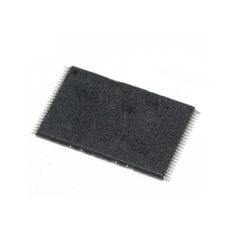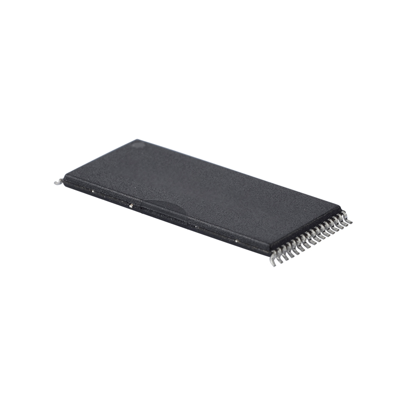
inventory:6,357
Infineon Technologies
TSOP-32
We are here to provide you with the electronic components you need!
Secure Code for Password Recovery via Email Request.
Please use the security code from your email to reset your password.
Please proceed to log in or return to the homepage.
LTC6957-1 is available from Analog Devices at Xecor. Designed for low phase noise signal buffering, driving, and logic level conversion, the LTC6957-1 offers optimized conversion of sine wave signals to logic levels, low additive jitter (45fsRMS), and a frequency range up to 300MHz. Available in multiple package options, including 12-Lead MSOP and 3mm × 3mm DFN, it is ideal for high-speed data acquisition, broadband wireless transceivers, medical imaging, and test and measurement applications. Whether used in system reference frequency distribution or military and secure radio systems, this series ensures high performance, low skew (3ps typical), and efficient operation for demanding applications. Xecor is an authorized distributor for Analog Devices. Please view our extensive selection of the LTC6957-1 series below.
| Part Number | Description | Package | Inventory | Add To Bom |
|---|---|---|---|---|
| LTC6957IMS-2#PBF | Dual output buffer and driver with LVDS outputs | MSOP-12 | 7,460 | |
| LTC6957HMS-1#PBF | Low phase noise clock buffer/divider providing multiple clean outputs with excellent jitter performance. | MSOP-12 | 5,932 | |
| LTC6957HMS-3#PBF | Experience precision timing with the powerful LTC6957HMS-3#PBF chip by Analog Devices | MSOP-12 | 7,172 | |
| LTC6957IDD-2#PBF | High-performance, dual-output buffer and driver with low phase noise | SON-12 | 9,160 | |
| LTC6957IDD-3#PBF | Clock Fanout Buffer 2-OUT 1-IN 1:2 12-Pin DFN EP Tube | SON-12 | 7,981 | |
| LTC6957IMS-3#PBF | Clock Fanout Buffer 2-OUT 1-IN 1:2 12-Pin MSOP Tube | MSOP-12 | 5,343 | |
| LTC6957HMS-2#PBF | Logic level translator with 1 channel in MSOP-12 package | MSOP-12 | 5,272 | |
| LTC6957IDD-1#PBF | Clock Fanout Buffer 2-OUT 1-IN 1:2 12-Pin DFN EP Tube | 12-WFDFNExposedPad | 7,032 | |
| LTC6957IMS-1#TRPBF | Ideal for applications requiring high-frequency signal amplification. | MSOP-12 | 5,701 | |
| LTC6957IMS-1#PBF | Low phase noise clock buffer and divider with multiple clean outputs for synchronization systems. | MSOP-12 | 4,699 | |
| LTC6957IDD-3#TRPBF | Outputs, 1 Input, 1 to 2 Ratio, 12-Pin DFN with Exposed Pad, Tape and Reel | DFN-12 | 6,218 | |
| LTC6957HMS-4#TRPBF | Streamline circuit design with integrated dual output functionality | MSOP-12 | 8,391 | |
| LTC6957HMS-1#TRPBF | LTC6957HMS-1#TRPBF: Enhance clock signal integrity | MSOP-12 | 6,002 | |
| LTC6957HMS-2#TRPBF | Single-input, dual-output clock buffer with low sk | MSOP-12 | 2,260 | |
| LTC6957HMS-4#PBF | Clock Fanout Buffer 2-OUT 1-IN 1:2 12-Pin MSOP Tube | MSOP-12 | 7,771 | |
| LTC6957IDD-2#TRPBF | Clock Fanout Buffer 2-OUT 1-IN 1:2 12-Pin DFN EP T/R | DFN-12 | 6,264 | |
| LTC6957IDD-1#TRPBF | Clock Fanout Buffer 2-OUT 1-IN 1:2 12-Pin DFN EP T/R | DFN-12 | 7,151 | |
| LTC6957IDD-4#PBF | Clock Fanout Buffer 2-OUT 1-IN 1:2 12-Pin DFN EP Tube | DFN-12 | 6,003 | |
| LTC6957IDD-4#TRPBF | Clock Fanout Buffer 2-OUT 1-IN 1:2 12-Pin DFN EP T/R | DFN-12 | 9,725 | |
| LTC6957IMS-3#TRPBF | Clock Fanout Buffer 2-OUT 1-IN 1:2 12-Pin MSOP T/R | MSOP-12 | 7,806 | |
| LTC6957IMS-2#TRPBF | Clock Fanout Buffer 2-OUT 1-IN 1:2 12-Pin MSOP T/R | MSOP-12 | 5,200 | |
| LTC6957IMS-4#PBF | Clock Fanout Buffer 2-OUT 1-IN 1:2 12-Pin MSOP Tube | MSOP-12 | 5,208 | |
| LTC6957IMS-4#TRPBF | Suitable for use with clocks or frequency generation circuits | MSOP-12 | 4,650 |