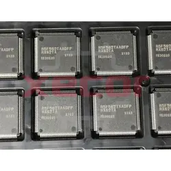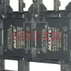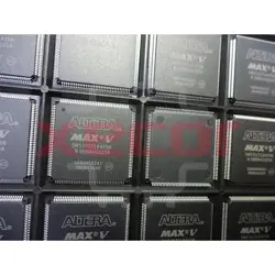
inventory:8,065
Amphenol
Plugin
We are here to provide you with the electronic components you need!
Secure Code for Password Recovery via Email Request.
Please use the security code from your email to reset your password.
Please proceed to log in or return to the homepage.

In Stock:8,720
XA7Z020-1CLG484Q is a high-quality System On Chip from AMD with a operating temperature range of - 40 C ~ + 125 C
Part Number : XA7Z020-1CLG484Q
Package/Case : CSBGA-484
Manufacturer : AMD
Components Classification : System On Chip
DataSheet : XA7Z020-1CLG484Q DataSheet (PDF)
Series : XA7Z020
The followings are basic parameters of the part selected concerning the characteristics of the part and categories it belongs to.
| Product Category | SoC FPGA | RoHS | Details |
| Mounting Style | SMD/SMT | Package / Case | CSBGA-484 |
| Core | ARM Cortex A9 | Number of Cores | 2 Core |
| Maximum Clock Frequency | 667 MHz | L1 Cache Instruction Memory | 2 x 32 kB |
| L1 Cache Data Memory | 2 x 32 kB | Number of Logic Elements | 85000 LE |
| Adaptive Logic Modules - ALMs | 13300 ALM | Embedded Memory | 4.9 Mbit |
| Number of I/Os | 130 I/O | Operating Supply Voltage | 1 V |
| Minimum Operating Temperature | - 40 C | Maximum Operating Temperature | + 125 C |
| Brand | Xilinx | Moisture Sensitive | Yes |
| Number of Logic Array Blocks - LABs | 6650 LAB | Product Type | Processors - Application Specialized |
| Series | XA7Z020 | Factory Pack Quantity | 1 |
| Subcategory | SOC - Systems on a Chip | Tradename | Zynq |
| Unit Weight | 2.696900 oz |
The Xilinx XA7Z020-1CLG484Q is a high-performance FPGA chip optimized for low-power and high-speed operations. It provides excellent performance for various applications, including analog and digital signal switching.
The XA7Z020-1CLG484Q pinout refers to the configuration and function of each pin in its CSBGA-484 package. This package typically includes a diagram showing the layout of the pins when viewed from the top down with pins named sequentially. Each pin on the XA7Z020-1CLG484Q has a specific role such as power supply input, ground connection, or signal interface. The pinout details are crucial for integrating this component into a circuit as they ensure correct connections for optimal device performance. Designers and engineers must refer to the datasheet provided by the manufacturer to get accurate information regarding each pin's function and electrical characteristics.
Advantages
Disadvantages
Q: What is the power consumption of the XA7Z020-1CLG484Q?
A: The power consumption of the XA7Z020-1CLG484Q depends on its operating frequency and voltage. Typically, it consumes around 0.5W to 2W.
Q: What is the maximum clock speed of the XA7Z020-1CLG484Q?
A: The maximum clock speed of the XA7Z020-1CLG484Q depends on its operating frequency and voltage. Typically, it can operate at a maximum clock speed of around 400MHz to 800MHz.
Q: What is the memory capacity of the XA7Z020-1CLG484Q?
A: The XA7Z020-1CLG484Q has on-chip memory including 4.5MB of block RAM and 180KB of UltraRAM.
Q: What is the thermal design power (TDP) of the XA7Z020-1CLG484Q?
A: The TDP of the XA7Z020-1CLG484Q depends on its operating frequency and voltage. Typically, it has a TDP of around 2W to 4W.
Warranty, Returns, and Additional Information
Parts Quality Guarantee: 365 days
Returns for refund: within 90 days
Returns for Exchange: within 90 days
Shipping:For example, FedEx, JP, UPS, DHL,SAGAWA, or YTC.
Parts Packaging Guarantee: Featuring 100% ESD anti-static protection, our packaging incorporates high toughness and superior buffering capabilities.
For example, channels like VISA,MasterCard,Western Union,PayPal,MoneyGram,Rakuten Pay and more.
If you have specific payment channel preferences or requirements, please get in touch with our sales team for assistance.
English expressions: Sort, Return, Sort, Gates
XC3S250E-4VQG100I is a versatile FPGA for development
Versatile integration of customizable logic functions
With ROHS compliance and a FBGA-676 package, this programmable logic device offers flexibility for CPLDs/FPGAs
The XC7K480T-2FFG1156I product is an advanced FPGA from the KINTEX-7 family, with 400 pins and FCBGA-1156 package
With its XC7K325T-2FFG900C design, this FPGA provides a high level of customization and performance for various applications
XC3S400A-4FTG256C features 770MHz operation
Reconfigurable hardware accelerator for various applications
32-bit Microcontroller for Motor Control
This product is sold in trays for convenient storage and transportation
PROGRAMMABLE LOGIC DEVICE EE PLD
FPGA Cyclone II Family with 4608 Cells
144-Pin TQFP CPLD MAX V Family 440 Macro Cells 118.3MHz 1.8V

ARM-ASeries 667MHz 256KB CSPBGA-484 Microcontroller Units
Inventory:
8,720
We provide an extended quality assurance period of 365 days for all components we offer. If a return or exchange becomes essential, kindly adhere to these guidelines:
·Initiate the request within 90 days after the item's shipment date.
·Coordinate the return or exchange with our team.
·Keep the items in their original condition as delivered.
·Please be aware that the feasibility of returning or exchanging items is contingent upon an evaluation of their actual state upon return.
We usually send out our orders during business days using FedEx, SF, UPS, or DHL. We're also here to assist with alternative shipping options. Should you require additional information about shipping particulars or expenses, please don't hesitate to get in touch with us.


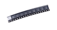
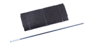
The items we ship will be packaged in anti-static bags, ensuring ESD anti-static protection, while the outer packaging boasts exceptional durability and sealing. We offer packaging options like Tape and Reel, Cut Tape, Tube, or Tray to suit your needs.

Accepted payment methods commonly encompass VISA, MasterCard, UnionPay, Western Union, PayPal, and various other options.
Should you have a particular payment preference or wish to seek information on rates and other specifics, please feel free to reach out to us.