inventory:7,978
Diodes Incorporated
SOIC-8
We are here to provide you with the electronic components you need!
Secure Code for Password Recovery via Email Request.
Please use the security code from your email to reset your password.
Please proceed to log in or return to the homepage.
In Stock:6,367
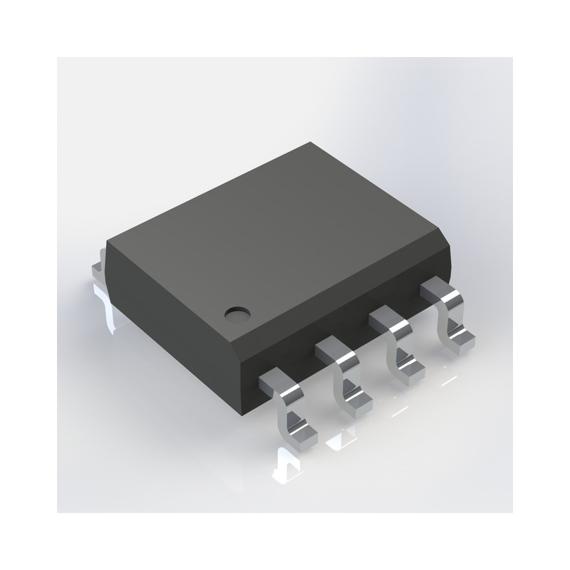
SI4925BDY-T1-E3 is a high-quality FET, MOSFET Arrays from VISHAY with a operating temperature range of - 55 C ~ + 150 C
Part Number : SI4925BDY-T1-E3
Package/Case : SOIC-8
Manufacturer : VISHAY
Components Classification : FET, MOSFET Arrays
DataSheet : SI4925BDY-T1-E3 DataSheet (PDF)
Series : SI4925
The followings are basic parameters of the part selected concerning the characteristics of the part and categories it belongs to.
| Product Category | MOSFET | RoHS | Details |
| REACH | Details | Technology | Si |
| Mounting Style | SMD/SMT | Package / Case | SOIC-8 |
| Transistor Polarity | P-Channel | Number of Channels | 2 Channel |
| Vds - Drain-Source Breakdown Voltage | 30 V | Id - Continuous Drain Current | 7.1 A |
| Rds On - Drain-Source Resistance | 25 mOhms | Vgs - Gate-Source Voltage | - 20 V, + 20 V |
| Vgs th - Gate-Source Threshold Voltage | 1 V | Qg - Gate Charge | 50 nC |
| Minimum Operating Temperature | - 55 C | Maximum Operating Temperature | + 150 C |
| Pd - Power Dissipation | 2 W | Channel Mode | Enhancement |
| Tradename | TrenchFET | Series | SI4 |
| Brand | Vishay Semiconductors | Configuration | Dual |
| Fall Time | 34 ns | Forward Transconductance - Min | 20 S |
| Height | 1.75 mm | Length | 4.9 mm |
| Product Type | MOSFET | Rise Time | 12 ns |
| Factory Pack Quantity | 2500 | Subcategory | MOSFETs |
| Transistor Type | 2 P-Channel | Typical Turn-Off Delay Time | 60 ns |
| Typical Turn-On Delay Time | 9 ns | Width | 3.9 mm |
| Part # Aliases | SI4925BDY-T1 | Unit Weight | 0.006596 oz |
The SI4925BDY-T1-E3 is a dual N-channel MOSFET (Metal-Oxide-Semiconductor Field-Effect Transistor) designed for high-power switching applications. This MOSFET features a low on-state resistance and high current handling capability, making it suitable for various power management tasks. (Note: The pin configuration below is a general representation. Refer to the specific datasheet for precise details.) Include a circuit diagram illustrating the connections and operation of the SI4925BDY-T1-E3 MOSFET for a visual representation. Note: For detailed technical specifications, please refer to the SI4925BDY-T1-E3 datasheet. Functionality The SI4925BDY-T1-E3 dual N-channel MOSFET is designed to facilitate high-current switching operations with low on-state resistance, ensuring efficient power management in various applications. Usage Guide For similar functionalities, consider these alternatives to the SI4925BDY-T1-E3:Overview of SI4925BDY-T1-E3
Pinout
Circuit Diagram
Key Features
Application
Equivalent
Warranty, Returns, and Additional Information
Parts Quality Guarantee: 365 days
Returns for refund: within 90 days
Returns for Exchange: within 90 days
Shipping:For example, FedEx, JP, UPS, DHL,SAGAWA, or YTC.
Parts Packaging Guarantee: Featuring 100% ESD anti-static protection, our packaging incorporates high toughness and superior buffering capabilities.
For example, channels like VISA,MasterCard,Western Union,PayPal,MoneyGram,Rakuten Pay and more.
If you have specific payment channel preferences or requirements, please get in touch with our sales team for assistance.
High power N-channel MOSFET for reliable switching applicatio
SI2323DS-T1-E3 is a P-type MOSFET with SOT-23 packaging
TO-220 package MOSFET with 220W power dissipation capability
Power Field-Effect Transistor
SI2303CDS-T1-GE3, P-channel MOSFET Transistor 1.9 A 30 V, 3-Pin SOT-23
SI2343CDS-T1-GE3 features a P-channel design and a 30-volt rating
MOSFET with P-Channel
F5-75R06KE3_B5 specifications
Trans GP BJT NPN 50V 1.5A 1000mW 3-Pin TO-39 Box
Ideal for switching and amplification circuits requiring low saturation voltage
Trans Darlington NPN 60V 10A 6000mW 3-Pin(2+Tab) TO-3 Tray
MOSFET 30V, N-Channel NexFET Power Mosfet
MATCHED PNP SMALL SIGNAL SURFACE MOUNT TRANSISTOR
Transistor MOSFET P-channel with a 30V voltage rating and a maximum current of 5.3A, packaged in an 8-pin SOIC
Inventory:
6,367
We provide an extended quality assurance period of 365 days for all components we offer. If a return or exchange becomes essential, kindly adhere to these guidelines:
·Initiate the request within 90 days after the item's shipment date.
·Coordinate the return or exchange with our team.
·Keep the items in their original condition as delivered.
·Please be aware that the feasibility of returning or exchanging items is contingent upon an evaluation of their actual state upon return.
We usually send out our orders during business days using FedEx, SF, UPS, or DHL. We're also here to assist with alternative shipping options. Should you require additional information about shipping particulars or expenses, please don't hesitate to get in touch with us.


The items we ship will be packaged in anti-static bags, ensuring ESD anti-static protection, while the outer packaging boasts exceptional durability and sealing. We offer packaging options like Tape and Reel, Cut Tape, Tube, or Tray to suit your needs.


Accepted payment methods commonly encompass VISA, MasterCard, UnionPay, Western Union, PayPal, and various other options.
Should you have a particular payment preference or wish to seek information on rates and other specifics, please feel free to reach out to us.