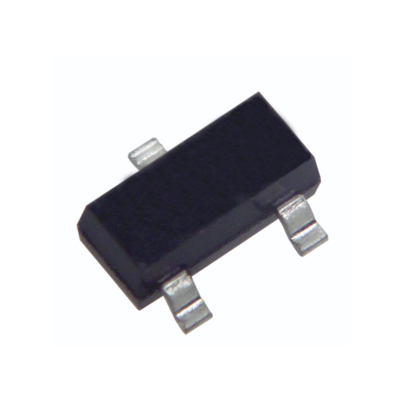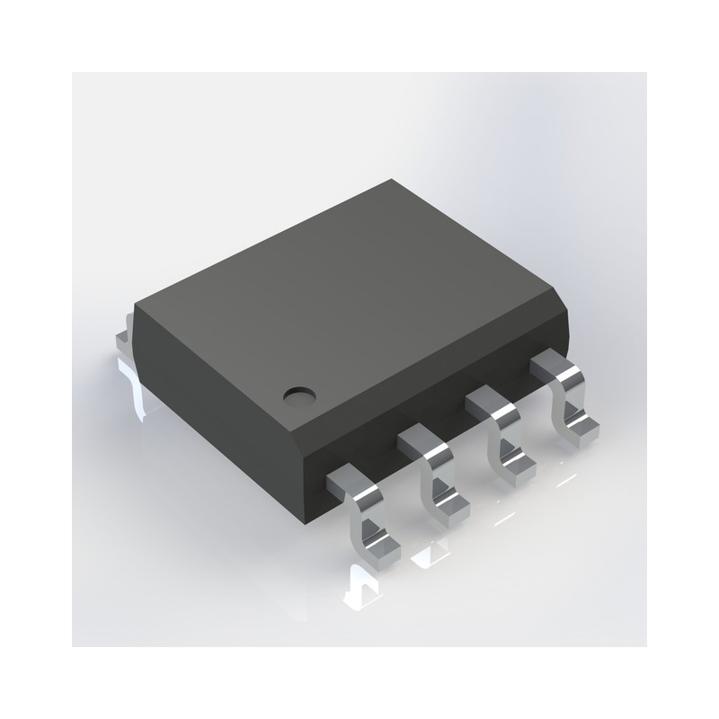
inventory:7,585
ADI
SOIC-8
We are here to provide you with the electronic components you need!
Secure Code for Password Recovery via Email Request.
Please use the security code from your email to reset your password.
Please proceed to log in or return to the homepage.

In Stock:8,792
JS28F128P33B85 is a high-quality Memory from Intel
Part Number : JS28F128P33B85
Other Name : JS28F128P33B85A
Package/Case : 56-TFSOP
Manufacturer : Intel
Components Classification : Memory
DataSheet : JS28F128P33B85 DataSheet (PDF)
Series : JS28F128P33
The followings are basic parameters of the part selected concerning the characteristics of the part and categories it belongs to.
| Series | StrataFlash™ | Package | Tray |
| Product Status | Obsolete | Programmabe | Not Verified |
| Memory Type | Non-Volatile | Memory Format | FLASH |
| Technology | FLASH - NOR | Memory Size | 128Mbit |
| Memory Organization | 8M x 16 | Memory Interface | Parallel |
| Clock Frequency | 40 MHz | Write Cycle Time - Word, Page | 85ns |
| Access Time | 85 ns | Voltage - Supply | 2.3V ~ 3.6V |
| Operating Temperature | -40°C ~ 85°C (TC) | Mounting Type | Surface Mount |
| Package / Case | 56-TFSOP (0.724", 18.40mm Width) | Supplier Device Package | 56-TSOP |
| Base Product Number | JS28F128P33 |
The JS28F128P33B85 is a flash memory chip optimized for high-speed and low-voltage operations. It provides excellent performance for embedded systems, automotive, industrial, networking, telecommunications, consumer electronics, medical devices, military and aerospace applications.
The JS28F128P33B85 pinout refers to the configuration and function of each pin in its 56-TFSOP (0.724", 18.40mm Width) package. This package typically includes a diagram showing the layout of the pins when viewed from the top down with pins named sequentially. Each pin on the JS28F128P33B85 has a specific role such as power supply input, ground connection, or signal interface. The pinout details are crucial for integrating this component into a circuit as they ensure correct connections for optimal device performance. Designers and engineers must refer to the datasheet provided by the manufacturer to get accurate information regarding each pin's function and electrical characteristics.
The JS28F128P33B85 offers several advantages, including high storage capacity, low power consumption, extended temperature range, fast random access time, and compatibility with parallel NOR flash interface. However, it also has some disadvantages, such as its relatively high cost compared to other flash memory chips.
The JS28F128P33B85 is equivalent to other flash memory chips that offer similar features and specifications. Some examples of equivalent products include the Micron MT29F512GABWC, the Samsung K9K8G8U0M, and the Toshiba TC58DVM6TAF.
Q: What is the storage capacity of the JS28F128P33B85?
A: The JS28F128P33B85 has a storage capacity of 128 megabytes.
Q: What is the power supply voltage of the JS28F128P33B85?
A: The JS28F128P33B85 operates at a power supply voltage of 3 volts.
Q: What is the random access time of the JS28F128P33B85?
A: The JS28F128P33B85 has a random access time of 85 nanoseconds.
Q: Is the JS28F128P33B85 compatible with parallel NOR flash interface?
A: Yes, the JS28F128P33B85 is compatible with the parallel NOR flash interface.
Warranty, Returns, and Additional Information
Parts Quality Guarantee: 365 days
Returns for refund: within 90 days
Returns for Exchange: within 90 days
Shipping:For example, FedEx, JP, UPS, DHL,SAGAWA, or YTC.
Parts Packaging Guarantee: Featuring 100% ESD anti-static protection, our packaging incorporates high toughness and superior buffering capabilities.
For example, channels like VISA,MasterCard,Western Union,PayPal,MoneyGram,Rakuten Pay and more.
If you have specific payment channel preferences or requirements, please get in touch with our sales team for assistance.
6 megabits by 8, 16-pin dual small outline integrated circuit package, Small outline integrated circuit with 16 pins, SOIC-16 package
density 16M x 16 configuration for efficient data storage
Featuring a cutting-edge SRAM configuration, this FBGA unit is designed for peak efficiency
SOIC package with 8-pin configuration
Altera EPC1PC8, 8-Pin PDIP Configuration Memory 16.7MHz
This product serves as a reliable storage solution for programming FPGA devices."
Configuration Memory PQFP100 16MX1 EPC16QC100N
64-Pin EBGA Package
Operating at frequencies up to 400kHz, this 24LC64T-I/OT EEPROM memory IC has a capacity of 64kb and supports I2C interface
Flash Memory 128Mb 3V 90ns Parallel NOR Flash
XCF08P - PROMs for In-System Programming of Platform Configurations
Supports Dual Supply Voltages (3.3V/1.8V)
512K x 16 Memory Array

128M-bit Capacity
Inventory:
8,792
We provide an extended quality assurance period of 365 days for all components we offer. If a return or exchange becomes essential, kindly adhere to these guidelines:
·Initiate the request within 90 days after the item's shipment date.
·Coordinate the return or exchange with our team.
·Keep the items in their original condition as delivered.
·Please be aware that the feasibility of returning or exchanging items is contingent upon an evaluation of their actual state upon return.
We usually send out our orders during business days using FedEx, SF, UPS, or DHL. We're also here to assist with alternative shipping options. Should you require additional information about shipping particulars or expenses, please don't hesitate to get in touch with us.


The items we ship will be packaged in anti-static bags, ensuring ESD anti-static protection, while the outer packaging boasts exceptional durability and sealing. We offer packaging options like Tape and Reel, Cut Tape, Tube, or Tray to suit your needs.


Accepted payment methods commonly encompass VISA, MasterCard, UnionPay, Western Union, PayPal, and various other options.
Should you have a particular payment preference or wish to seek information on rates and other specifics, please feel free to reach out to us.