inventory:8,580
TI
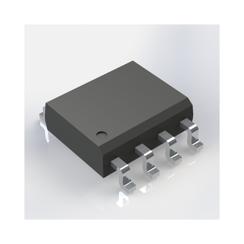
SOIC (D)-8
We are here to provide you with the electronic components you need!
Secure Code for Password Recovery via Email Request.
Please use the security code from your email to reset your password.
Please proceed to log in or return to the homepage.

In Stock:7,893
5CGTFD5C5F27C7N is a high-quality FPGAs from Altera featuring a supply voltage of 1.1 V with a operating temperature range of 0 C ~ + 85 C
Part Number : 5CGTFD5C5F27C7N
Package/Case : BGA-672
Manufacturer : Altera
Components Classification : FPGAs
DataSheet : 5CGTFD5C5F27C7N DataSheet (PDF)
Series : 5CGTFD5C
The followings are basic parameters of the part selected concerning the characteristics of the part and categories it belongs to.
| Product Category | FPGA - Field Programmable Gate Array | RoHS | Details |
| REACH | Details | Series | 5CGTFD5C |
| Number of Logic Elements | 77000 LE | Adaptive Logic Modules - ALMs | 29080 ALM |
| Embedded Memory | 4.884 Mbit | Number of I/Os | 336 I/O |
| Supply Voltage - Max | 1.1 V | Minimum Operating Temperature | 0 C |
| Maximum Operating Temperature | + 85 C | Data Rate | 6.144 Gb/s |
| Number of Transceivers | 6 Transceiver | Mounting Style | SMD/SMT |
| Package / Case | FBGA-672 | Brand | Altera |
| Embedded Block RAM - EBR | 424 kbit | Maximum Operating Frequency | 925 MHz |
| Moisture Sensitive | Yes | Number of Logic Array Blocks - LABs | 2908 LAB |
| Operating Supply Voltage | 1.1 V | Product Type | FPGA - Field Programmable Gate Array |
| Factory Pack Quantity | 40 | Subcategory | Programmable Logic ICs |
| Total Memory | 4884 kbit | Tradename | Cyclone V |
| Part # Aliases | 968902 | Unit Weight | 0.758454 oz |
The 5CGTFD5C5F27C7N is a Field-Programmable Gate Array (FPGA) integrated circuit featuring advanced programmable logic capabilities and built-in memory blocks. This FPGA is designed for high-performance applications requiring custom logic implementations and flexible configuration options. (Note: The pin configuration below is a general representation. Refer to the specific datasheet for precise details.) Include a circuit diagram illustrating the connections and operation of the 5CGTFD5C5F27C7N FPGA for a visual representation. Note: For detailed technical specifications, please refer to the 5CGTFD5C5F27C7N datasheet. Functionality The 5CGTFD5C5F27C7N FPGA offers unparalleled flexibility in designing and implementing custom logic functions. It provides a versatile platform for addressing complex digital processing tasks with ease. Usage Guide Q: What tools are recommended for programming the 5CGTFD5C5F27C7N FPGA? Q: Can the 5CGTFD5C5F27C7N be reprogrammed multiple times? For similar functionalities, consider these alternatives to the 5CGTFD5C5F27C7N:Overview of 5CGTFD5C5F27C7N
Pinout
Circuit DiagramKey Features
Application
Frequently Asked Questions
A: Popular FPGA development tools such as Quartus Prime or Vivado are commonly used for programming and configuring FPGAs like the 5CGTFD5C5F27C7N.
A: Yes, FPGAs are designed for reprogramming, allowing users to change the logic configuration multiple times as needed.Equivalent
Warranty, Returns, and Additional Information
Parts Quality Guarantee: 365 days
Returns for refund: within 90 days
Returns for Exchange: within 90 days
Shipping:For example, FedEx, JP, UPS, DHL,SAGAWA, or YTC.
Parts Packaging Guarantee: Featuring 100% ESD anti-static protection, our packaging incorporates high toughness and superior buffering capabilities.
For example, channels like VISA,MasterCard,Western Union,PayPal,MoneyGram,Rakuten Pay and more.
If you have specific payment channel preferences or requirements, please get in touch with our sales team for assistance.
Altera FPGA EP2C35F484C8N, Cyclone II 33216 Cells, 33216 Blocks, 484-Pin FBGA
Product EP3C5F256C8N description: FPGA Cyclone® III Family 5136 Cells 402MHz 65nm Technology 1.2V 256-Pin TFBGA
Cyclone IV GX FPGA with 30K logic elements and transceivers. Cost-effective for embedded interface designs.
EP4CE115F29I7N is a adaptable logic device ideal for a variety of applications due to its programmable nature
256UBGA IC FPGA with 150 I/o
PBGA484 Field Programmable Gate Array featuring 301000 Cells in CMOS
Field Programmable Gate Array with 392 LABs and 91 IOs
Reconfigurable hardware accelerator for various applications
32-bit Microcontroller for Motor Control
This product is sold in trays for convenient storage and transportation
PROGRAMMABLE LOGIC DEVICE EE PLD
FPGA Cyclone II Family with 4608 Cells
144-Pin TQFP CPLD MAX V Family 440 Macro Cells 118.3MHz 1.8V

28nm technology
Inventory:
7,893
We provide an extended quality assurance period of 365 days for all components we offer. If a return or exchange becomes essential, kindly adhere to these guidelines:
·Initiate the request within 90 days after the item's shipment date.
·Coordinate the return or exchange with our team.
·Keep the items in their original condition as delivered.
·Please be aware that the feasibility of returning or exchanging items is contingent upon an evaluation of their actual state upon return.
We usually send out our orders during business days using FedEx, SF, UPS, or DHL. We're also here to assist with alternative shipping options. Should you require additional information about shipping particulars or expenses, please don't hesitate to get in touch with us.


The items we ship will be packaged in anti-static bags, ensuring ESD anti-static protection, while the outer packaging boasts exceptional durability and sealing. We offer packaging options like Tape and Reel, Cut Tape, Tube, or Tray to suit your needs.


Accepted payment methods commonly encompass VISA, MasterCard, UnionPay, Western Union, PayPal, and various other options.
Should you have a particular payment preference or wish to seek information on rates and other specifics, please feel free to reach out to us.