
inventory:8,065
Amphenol
Plugin
We are here to provide you with the electronic components you need!
Secure Code for Password Recovery via Email Request.
Please use the security code from your email to reset your password.
Please proceed to log in or return to the homepage.
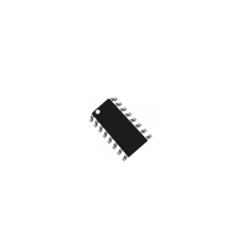
12 Megabits capacity, Multi-Chip Package support, uniform 4 kilobyte sectors and Dual/Quad SPI communication
Inventory:1,000
As embedded systems become increasingly sophisticated, the demand for higher-capacity, faster, and more compact memory solutions continues to grow. Modern electronic devices often require substantial storage space for firmware, operating systems, graphical interfaces, configuration files, and other critical data.
The W25M512JVFIQ is a high-density SpiStack Flash memory solution designed for applications that require large storage capacity while maintaining a compact PCB footprint. With its stacked memory architecture and flexible SPI interface options, this device is well suited for a wide range of embedded and industrial applications.
The W25M512JVFIQ is part of the Winbond W25M-JV SpiStack Flash family. It combines two 256Mb NOR Flash memory dies within a single package, providing a total memory capacity of 512Mb.
The stacked architecture enables designers to achieve higher memory density without significantly increasing board space. This can be particularly beneficial for compact electronic products where PCB area is limited.
The device supports multiple serial communication modes, including standard SPI, Dual SPI, and Quad SPI, offering flexibility for different system architectures and performance requirements.
| Feature | Specification |
|---|---|
| Part Number | W25M512JVFIQ |
| Total Memory Capacity | 512Mb |
| Memory Configuration | 256Mb + 256Mb NOR Flash |
| Interface | SPI / Dual SPI / Quad SPI |
| Maximum Frequency | Up to 104MHz |
| Operating Voltage | 2.7V to 3.6V |
| Operating Temperature | -40°C to +85°C |
| Package Type | SOP-16 |
| Package Width | 300 mil |
These specifications make the W25M512JVFIQ a suitable option for embedded systems requiring high-density non-volatile memory and efficient serial data access.
Modern embedded devices require significantly more memory than earlier generations of electronic products. Firmware has become increasingly complex, while graphical user interfaces, communication protocols, security features, and system updates continue to increase storage requirements.
The 512Mb capacity of the W25M512JVFIQ provides additional space for a variety of applications, including:
By integrating two memory dies into a single package, the SpiStack architecture can help designers increase memory capacity while simplifying PCB layouts.
Data transfer speed is an important consideration when selecting Flash memory for embedded applications.
The W25M512JVFIQ supports standard SPI as well as Dual SPI and Quad SPI communication modes. These interface options allow system designers to select an appropriate balance between hardware compatibility and data transfer performance.
Quad SPI, in particular, enables data transmission across multiple I/O lines, which can improve throughput compared with traditional single-bit SPI communication.
This flexibility makes the W25M512JVFIQ compatible with a variety of microcontrollers, processors, and other embedded platforms that support serial Flash memory.
PCB space is a valuable resource in many modern electronic products. Portable devices, industrial controllers, consumer electronics, and compact communication systems often require designers to maximize functionality within limited board dimensions.
The SpiStack architecture used in the W25M512JVFIQ addresses this challenge by integrating multiple Flash memory dies into one package.
Key advantages of this approach may include:
For designs that require substantial non-volatile memory without using multiple discrete Flash components, a stacked memory solution can offer important practical benefits.
Thanks to its high storage capacity and flexible serial interface, the W25M512JVFIQ can be considered for various electronic applications.
Industrial equipment often requires reliable storage for firmware, operating software, system configurations, and application data. High-capacity serial Flash can support increasingly complex industrial control platforms.
Portable electronic devices typically have strict PCB space limitations. A high-density Flash solution in a compact package can help designers optimize available board space.
Point-of-sale systems may require significant storage capacity for operating software, application programs, configuration data, and security-related firmware.
Monitoring systems and smart electronic terminals may need to store large firmware packages and application resources. High-speed serial Flash can support efficient data access in these systems.
Embedded computing systems frequently require external non-volatile memory for boot code, firmware, applications, and system data. The W25M512JVFIQ provides a high-capacity option for such applications.
When integrating the W25M512JVFIQ into an electronic system, engineers should consider several important design factors.
The device operates within a 2.7V to 3.6V voltage range. A stable power supply and appropriate decoupling capacitors are important for reliable system operation.
The selected microcontroller or processor should support the required SPI, Dual SPI, or Quad SPI communication mode.
For high-speed serial communication, signal routing should be carefully designed. Short signal paths and appropriate power and ground connections can help maintain signal integrity.
System software must correctly support the Flash memory architecture and associated read, program, and erase operations.
Before PCB production, engineers should verify the package dimensions, land pattern, and assembly requirements to ensure compatibility with the hardware design.
Selecting Flash memory involves more than simply choosing the highest available storage capacity. Engineers should evaluate multiple factors, including:
The right memory solution should match both the technical requirements and the long-term goals of the product design.
The W25M512JVFIQ is a high-density SpiStack Flash memory solution that combines two 256Mb NOR Flash memory dies to provide a total capacity of 512Mb. With support for SPI, Dual SPI, and Quad SPI communication modes, it offers flexibility for a wide range of embedded system architectures.
Its compact package, high storage density, and broad operating temperature range make it a potential solution for industrial control systems, handheld devices, POS terminals, monitoring equipment, and other embedded applications.
For engineers developing products that require substantial non-volatile memory while minimizing PCB space requirements, the W25M512JVFIQ is a component worth considering. Before final component selection, designers should always review the latest manufacturer datasheet and verify all electrical, timing, package, and application-specific requirements.
The W25M512JVFIQ can be used in industrial control systems, POS terminals, monitoring equipment, handheld devices, and other embedded applications. Its high memory capacity makes it suitable for storing firmware, application code, configuration data, and other non-volatile information.
The W25M512JVFIQ Flash memory supports standard SPI, Dual SPI, and Quad SPI communication modes. These flexible interface options allow designers to select the appropriate data transfer method based on the performance and compatibility requirements of their embedded systems.
The W25M512JVFIQ is a high-density 512Mb SpiStack NOR Flash memory device designed for embedded systems and electronic applications. Its stacked memory architecture helps provide large storage capacity while reducing the PCB space required for multiple discrete memory devices.



 Dr. James Anderson


Still, need help? Contact Us: [email protected]