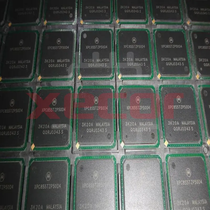
XPC855TZP50D4
Microprocessors - MPU
Inventory:5,814
- 90-day after-sales guarantee
- 365 Days Quality Guarantee
- Genuine Product Guarantee
- 7*24 hours service quarantee
-
Part Number : XPC855TZP50D4
-
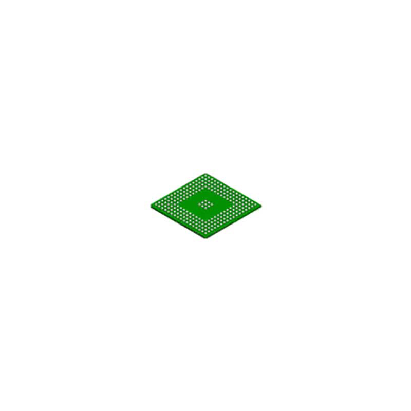
Package/Case : PBGA-357
-
Brands : MOTOROLA INC
-
Components Categories : Microprocessors - MPU
-
Datesheet : XPC855TZP50D4 DataSheet (PDF)
Overview of XPC855TZP50D4
Key Features
- The following list summarizes the key MPC860 features:
- Embedded single-issue, 32-bit MPC8xx core (implementing the PowerPC architecture) with thirty-two 32-bit general-purpose registers (GPRs)
- — The core performs branch prediction with conditional prefetch, without conditional execution
- — 4- or 8-Kbyte data cache and 4- or 16-Kbyte instruction cache (see Table 1)
- – 16-Kbyte instruction caches are four-way, set-associative with 256 sets;
- 4-Kbyte instruction caches are two-way, set-associative with 128 sets.
- – 8-Kbyte data caches are two-way, set-associative with 256 sets; 4-Kbyte data caches are two-way, set-associative with 128 sets.
- – Cache coherency for both instruction and data caches is maintained on 128-bit (4-word) cache blocks.
- – Caches are physically addressed, implement a least recently used (LRU) replacement algorithm, and are lockable on a cache block basis.
- — Instruction and data caches are two-way, set-associative, physically addressed, LRU replacement, and lockable on-line granularity.
- — MMUs with 32-entry TLB, fully associative instruction, and data TLBs
- — MMUs support multiple page sizes of 4, 16, and 512 Kbytes, and 8 Mbytes; 16 virtual address spaces and 16 protection groups
- — Advanced on-chip-emulation debug mode
- Up to 32-bit data bus (dynamic bus sizing for 8, 16, and 32 bits)
- 32 address lines
- Operates at up to 80 MHz
- Memory controller (eight banks)
- — Contains complete dynamic RAM (DRAM) controller
- — Each bank can be a chip select or RASto support a DRAM bank
- — Up to 15 wait states programmable per memory bank
- — Glueless interface to DRAM, SIMMS, SRAM, EPROM, Flash EPROM, and other memory devices.
- — DRAM controller programmable to support most size and speed memory interfaces
- — Four CASlines, four WElines, one OEline
- — Boot chip-select available at reset (options for 8-, 16-, or 32-bit memory)
- — Variable block sizes (32 Kbyte to 256 Mbyte)
- — Selectable write protection
- — On-chip bus arbitration logic
- General-purpose timers
- — Four 16-bit timers or two 32-bit timers
- — Gate mode can enable/disable counting
- — Interrupt can be masked on reference match and event capture
- System integration unit (SIU)
- — Bus monitor
- — Software watchdog
- — Periodic interrupt timer (PIT)
- — Low-power stop mode
- — Clock synthesizer
- — Three parallel I/O registers with open-drain capability
- Four baud-rate generators (BRGs)
- — Independent (can be connected to any SCC or SMC)
- — Allow changes during operation
- — Autobaud support option
- Four serial communications controllers (SCCs)
- — Ethernet/IEEE 802.3 optional on SCC1–4, supporting full 10-Mbps operation (available only on specially programmed devices).
- — HDLC/SDLC(all channels supported at 2 Mbps)
- — HDLC bus (implements an HDLC-based local area network (LAN))
- — Asynchronous HDLC to support PPP (point-to-point protocol)
- — AppleTalk
- — Universal asynchronous receiver transmitter (UART)
- — Synchronous UART
- — Serial infrared (IrDA)
- — Binary synchronous communication (BISYNC)
- — Totally transparent (bit streams)
- — Totally transparent (frame based with optional cyclic redundancy check (CRC))
- Two SMCs (serial management channels)
- — UART
- — Transparent
- — General circuit interface (GCI) controller
- — Can be connected to the time-division multiplexed (TDM) channels
- One SPI (serial peripheral interface)
- — Supports master and slave modes
- — Supports multimaster operation on the same bus
- One I2C (inter-integrated circuit) port
- — Supports master and slave modes
- — Multiple-master environment support
- Time-slot assigner (TSA)
- — Allows SCCs and SMCs to run in multiplexed and/or non-multiplexed operation
- — Supports T1, CEPT, PCM highway, ISDN basic rate, ISDN primary rate, user defined
- — 1- or 8-bit resolution
- — Allows independent transmit and receive routing, frame synchronization, clocking
- — Allows dynamic changes
- — Can be internally connected to six serial channels (four SCCs and two SMCs)
- Parallel interface port (PIP)
- — Centronics interface support
- — Supports fast connection between compatible ports on the MPC860 or the MC68360
- PCMCIA interface
- — Master (socket) interface, release 2.1 compliant
- — Supports two independent PCMCIA sockets
- — Eight memory or I/O windows supported
- Low power support
- — Full on—all units fully powered
- — Doze—core functional units disabled, except time base decrementer, PLL, memory controller, RTC, and CPM in low-power standby
- — Sleep—all units disabled, except RTC and PIT, PLL active for fast wake up
- — Deep sleep—all units disabled including PLL, except RTC and PIT
- — Power down mode— all units powered down, except PLL, RTC, PIT, time base, and decrementer
- Debug interface
- — Eight comparators: four operate on instruction address, two operate on data address, and two operate on data
- — Supports conditions: =≠<>
- — Each watchpoint can generate a break-point internally
- 3.3 V operation with 5-V TTL compatibility except EXTAL and EXTCLK
- 357-pin ball grid array (BGA) package
Specifications
The followings are basic parameters of the part selected concerning the characteristics of the part and categories it belongs to.
| Rohs Code | No | Part Life Cycle Code | Transferred |
| Ihs Manufacturer | MOTOROLA INC | Package Description | PLASTIC, BGA-357 |
| Reach Compliance Code | ECCN Code | 3A991.A.2 | |
| HTS Code | 8542.31.00.01 | Address Bus Width | 32 |
| Bit Size | 32 | Boundary Scan | YES |
| Clock Frequency-Max | 50 MHz | External Data Bus Width | 32 |
| Format | FIXED POINT | Integrated Cache | YES |
| JESD-30 Code | S-PBGA-B357 | Length | 25 mm |
| Low Power Mode | YES | Number of Terminals | 357 |
| Operating Temperature-Min | Package Body Material | PLASTIC/EPOXY | |
| Package Code | BGA | Package Equivalence Code | BGA357,19X19,50 |
| Package Shape | SQUARE | Package Style | GRID ARRAY |
| Power Supplies | 3.3 V | Qualification Status | Not Qualified |
| Seated Height-Max | 2.05 mm | Speed | 50 MHz |
| Supply Voltage-Max | 3.465 V | Supply Voltage-Min | 3.135 V |
| Supply Voltage-Nom | 3.3 V | Surface Mount | YES |
| Technology | CMOS | Terminal Form | BALL |
| Terminal Pitch | 1.27 mm | Terminal Position | BOTTOM |
| Width | 25 mm | uPs/uCs/Peripheral ICs Type | MICROPROCESSOR, RISC |
Warranty & Returns
Warranty, Returns, and Additional Information
-
QA & Return Policy
Parts Quality Guarantee: 365 days
Returns for refund: within 90 days
Returns for Exchange: within 90 days
-
Shipping and Package
Shipping:For example, FedEx, SF, UPS, or DHL.UPS, or DHL.
Parts Packaging Guarantee: Featuring 100% ESD anti-static protection, our packaging incorporates high toughness and superior buffering capabilities.
-
Payment
For example, channels like VISA, MasterCard, UnionPay, Western Union, PayPal, and more.
If you have specific payment channel preferences or requirements, please get in touch with our sales team for assistance.
Similar Product
XPC860TZP50D4
MPU PowerQUICC MPC8xx Processor RISC 32bit 0.32um 50MHz 357-Pin BGA
MAXP-37161B
Analog & Digital Crosspoint ICs
L99PM72PXP
Power Management Specialized - PMIC Advanced pwr manage IC supporting CAN
L99PM62XP
Power Management IC 6V to 18V Automotive AEC-Q100 36-Pin PowerSSO EP Tube
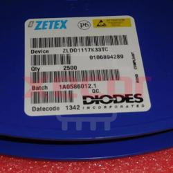
ZLDO1117K33TC
The ZLDO1117K33TC low dropout regulator is housed in a TO252 package and can supply a maximum current of 1A at an output voltage of 3.3V
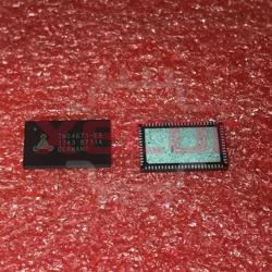
TMC4671-ES
TMC4671-ES is a gate-driver, microcontroller, and motion controller for 3-phase BLDC/PMSM motors.
FMS6141S5X
Optimize your video feed for seamless integration with other equipment through the advanced features of the FMS6141S5X
MCIMX515DJM8C
MAPBGA 529 i.MX51 MPU featuring an 800MHz ARM Cortex-A8 core