
XCL202B181BR-G
Switching Voltage Regulators RECOMMENDED ALT 865-XCL202B181ER-G
| Quantity | Unit Price(USD) | Ext. Price |
|---|---|---|
| 1 | $3.441 | $3.44 |
| 200 | $1.373 | $274.60 |
| 500 | $1.328 | $664.00 |
| 1000 | $1.305 | $1,305.00 |
Inventory:5,518
- 90-day after-sales guarantee
- 365 Days Quality Guarantee
- Genuine Product Guarantee
- 7*24 hours service quarantee
-
Part Number : XCL202B181BR-G
-
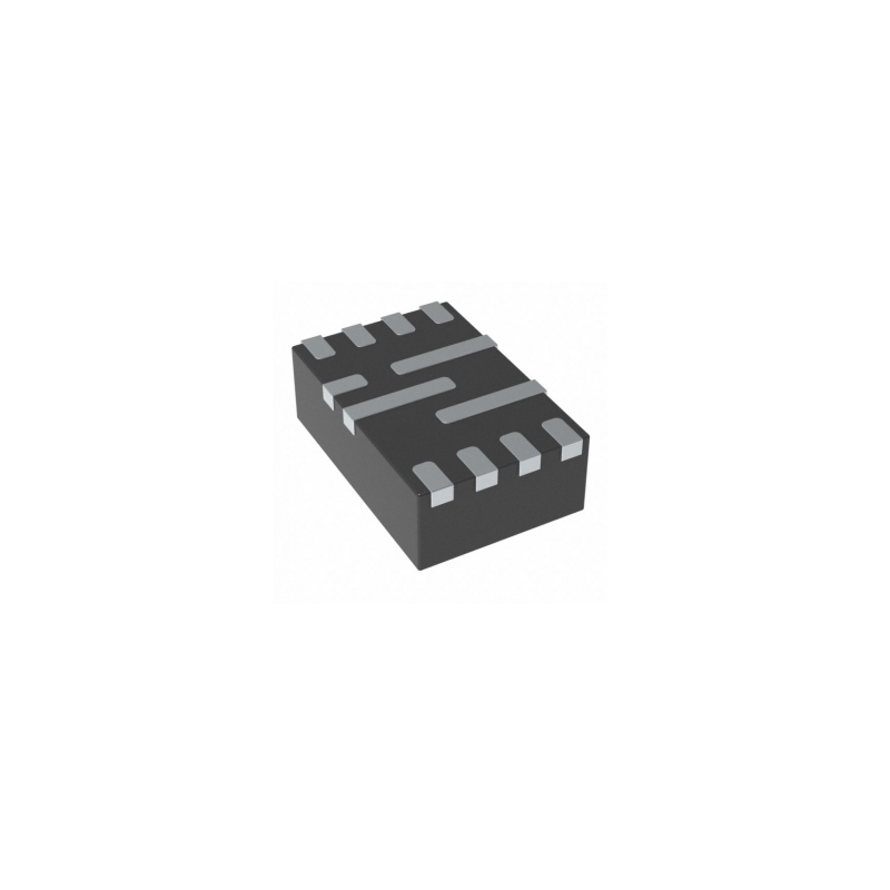
Package/Case : CL-2025
-
Brands : Torex Semiconductor Ltd
-
Components Categories : DC DC Converters
-
Datesheet : XCL202B181BR-G DataSheet (PDF)
The XCL202B181BR-G is a step-down voltage regulator IC that features high efficiency and a wide input voltage range. It is designed to provide a regulated output voltage from a higher input voltage source, making it suitable for various power management applications. (Note: The pin configuration below is a general representation. Refer to the specific datasheet for precise details.) Include a circuit diagram illustrating the connections and operation of the XCL202B181BR-G IC for a visual representation. Note: For detailed technical specifications, please refer to the XCL202B181BR-G datasheet. Functionality The XCL202B181BR-G is a step-down voltage regulator that efficiently converts higher input voltages to regulated lower output voltages. It ensures stable power supply for electronic devices. Usage Guide Q: What is the typical efficiency of the XCL202B181BR-G? Q: Is the XCL202B181BR-G suitable for automotive applications? For similar functionalities, consider these alternatives to the XCL202B181BR-G:Overview of XCL202B181BR-G
Pinout
Circuit Diagram
Key Features
Application
Frequently Asked Questions
A: The XCL202B181BR-G offers a typical efficiency of over 90%, providing high power conversion efficiency.
A: Yes, the XCL202B181BR-G can withstand automotive operating conditions and is suitable for automotive power management applications.Equivalent
Specifications
The followings are basic parameters of the part selected concerning the characteristics of the part and categories it belongs to.
| Rohs Code | Yes | Part Life Cycle Code | Active |
| Ihs Manufacturer | TOREX SEMICONDUCTOR LTD | Package Description | QCCN, LCC8(UNSPEC) |
| Reach Compliance Code | compliant | ECCN Code | EAR99 |
| HTS Code | 8542.39.00.01 | Samacsys Manufacturer | Torex |
| Additional Feature | PFM CONTROL TECHNIQUE ALSO AVAILABLE | Analog IC - Other Type | SWITCHING REGULATOR |
| Control Mode | CURRENT-MODE | Control Technique | PULSE WIDTH MODULATION |
| Input Voltage-Max | 6 V | Input Voltage-Min | 2 V |
| Input Voltage-Nom | 4.2 V | JESD-30 Code | R-XQCC-N8 |
| Length | 2.5 mm | Moisture Sensitivity Level | 1 |
| Number of Functions | 1 | Number of Terminals | 8 |
| Operating Temperature-Max | 85 °C | Operating Temperature-Min | -40 °C |
| Output Current-Max | 0.4 A | Output Voltage-Max | 1.836 V |
| Output Voltage-Min | 1.764 V | Output Voltage-Nom | 1.8 V |
| Package Body Material | UNSPECIFIED | Package Code | HQCCN |
| Package Equivalence Code | LCC8,0.08X0.1(UNSPEC) | Package Shape | RECTANGULAR |
| Package Style | CHIP CARRIER, HEAT SINK/SLUG | Peak Reflow Temperature (Cel) | 260 |
| Qualification Status | Not Qualified | Seated Height-Max | 1.04 mm |
| Supply Current-Max (Isup) | 0.033 mA | Surface Mount | YES |
| Switcher Configuration | BUCK | Switching Frequency-Max | 1380 kHz |
| Temperature Grade | INDUSTRIAL | Terminal Finish | NICKEL SILVER GOLD |
| Terminal Form | NO LEAD | Terminal Pitch | 0.55 mm |
| Terminal Position | QUAD | Time@Peak Reflow Temperature-Max (s) | 10 |
| Width | 2 mm | Series | XCL202 |
| Package | Tape & Reel (TR) | Product Status | Not For New Designs |
| Type | Non-Isolated PoL Module | Number of Outputs | 1 |
| Voltage - Input (Min) | 2V | Voltage - Input (Max) | 6V |
| Voltage - Output 1 | 1.8V | Current - Output (Max) | 400mA |
| Applications | ITE (Commercial) | Features | SCP, UVLO |
| Operating Temperature | -40°C ~ 85°C | Efficiency | 92% |
| Mounting Type | Surface Mount | Package / Case | 6-TDFN Exposed Pad |
| Size / Dimension | 0.10" L x 0.08" W x 0.04" H (2.5mm x 2.0mm x 1.0mm) | Supplier Device Package | CL-2025 |
| Base Product Number | XCL202 |
Warranty & Returns
Warranty, Returns, and Additional Information
-
QA & Return Policy
Parts Quality Guarantee: 365 days
Returns for refund: within 90 days
Returns for Exchange: within 90 days
-
Shipping and Package
Shipping:For example, FedEx, SF, UPS, or DHL.UPS, or DHL.
Parts Packaging Guarantee: Featuring 100% ESD anti-static protection, our packaging incorporates high toughness and superior buffering capabilities.
-
Payment
For example, channels like VISA, MasterCard, UnionPay, Western Union, PayPal, and more.
If you have specific payment channel preferences or requirements, please get in touch with our sales team for assistance.
Similar Product
XCL220B123FR-G
Switching Voltage Regulators 1A Indct / Stp Dwn Micro DCDC Converter

XCL206B123CR-G
Conv DC-DC Single Step Down 2V to 6V 8-Pin CL-2025-02 T/R
XCL206B333AR-G
Recommended Alternative for XCL206B333AR-G Switching Voltage Regulator 865-XCL206B333CR-G
XCL206B183CR-G
Switching Voltage Regulators 600mA Inductor DCDC Converter

XCL206B183AR-G
Switching Voltage Regulators RECOMMENDED ALT 865-XCL206B183CR-G
XCL214B123DR
Switching Voltage Regulators 1.5A Inductor DCDC Converter
XCL219B183FR-G
Switching Voltage Regulators 1A Indct / Stp Dwn Micro DCDC Converter
XCL220B183FR-G
Switching Voltage Regulators 1A Indct / Stp Dwn Micro DCDC Converter