
XC7K325T-2FFG900C
XILINX - XC7K325T-2FFG900C - FPGA, KIntex-7, MMCM, PLL, 400 I/O's, 470.37 MHz, 326080 Cells, 970 mV to 1.03 V, FCBGA-900
Inventory:6,214
- 90-day after-sales guarantee
- 365 Days Quality Guarantee
- Genuine Product Guarantee
- 7*24 hours service quarantee
-
Part Number : XC7K325T-2FFG900C
-
Package/Case : BGA
-
Brands : Xilinx
-
Components Categories : FPGAs (Field Programmable Gate Array)
-
Datesheet : XC7K325T-2FFG900C DataSheet (PDF)
The XC7K325T-2FFG900C is a Xilinx Kintex-7 FPGA featuring a -2 speed grade and FFG package option. This FPGA offers a high-performance, low-power solution for a wide range of applications, including communication systems, industrial automation, and image processing. (Note: The pin configuration below is a general representation. Refer to the specific datasheet for precise details.) Include a circuit diagram illustrating the connections and operation of the XC7K325T-2FFG900C FPGA for a visual representation. Note: For detailed technical specifications, please refer to the XC7K325T-2FFG900C datasheet. Functionality The XC7K325T-2FFG900C FPGA delivers high-speed data processing and signal handling capabilities, making it a versatile solution for various applications requiring FPGA implementation. Usage Guide Q: What programming tools are recommended for configuring the XC7K325T-2FFG900C? Q: Is the XC7K325T-2FFG900C suitable for high-temperature environments? For similar FPGA solutions, consider these alternatives to the XC7K325T-2FFG900C:Overview of XC7K325T-2FFG900C
Pinout
Circuit Diagram
Key Features
Application
Frequently Asked Questions
A: Xilinx Vivado Design Suite is commonly used for FPGA programming and configuration.
A: The FFG package option provides enhanced thermal performance, enabling operation in high-temperature environments with proper cooling measures.Equivalent
Specifications
The followings are basic parameters of the part selected concerning the characteristics of the part and categories it belongs to.
| Product Category | FPGA - Field Programmable Gate Array | RoHS | Details |
| Series | XC7K325T | Number of Logic Elements | 326080 LE |
| Adaptive Logic Modules - ALMs | 50950 ALM | Embedded Memory | 15.64 Mbit |
| Number of I/Os | 500 I/O | Supply Voltage - Min | 970 mV |
| Supply Voltage - Max | 1.03 V | Minimum Operating Temperature | 0 C |
| Maximum Operating Temperature | + 85 C | Data Rate | 12.5 Gb/s |
| Number of Transceivers | 16 Transceiver | Mounting Style | SMD/SMT |
| Package / Case | FBGA-900 | Brand | Xilinx |
| Distributed RAM | 4000 kbit | Embedded Block RAM - EBR | 16020 kbit |
| Maximum Operating Frequency | 640 MHz | Moisture Sensitive | Yes |
| Number of Logic Array Blocks - LABs | 25475 LAB | Operating Supply Voltage | 1.2 V to 3.3 V |
| Product Type | FPGA - Field Programmable Gate Array | Factory Pack Quantity | 1 |
| Subcategory | Programmable Logic ICs | Tradename | Kintex |
| Unit Weight | 8.810554 oz |
Warranty & Returns
Warranty, Returns, and Additional Information
-
QA & Return Policy
Parts Quality Guarantee: 365 days
Returns for refund: within 90 days
Returns for Exchange: within 90 days
-
Shipping and Package
Shipping:For example, FedEx, SF, UPS, or DHL.UPS, or DHL.
Parts Packaging Guarantee: Featuring 100% ESD anti-static protection, our packaging incorporates high toughness and superior buffering capabilities.
-
Payment
For example, channels like VISA, MasterCard, UnionPay, Western Union, PayPal, and more.
If you have specific payment channel preferences or requirements, please get in touch with our sales team for assistance.
Similar Product
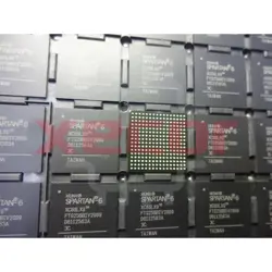
XC6SLX9-3FTG256C
Small and versatile FPGA
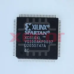
XCS10XL-4VQ100C
96-Cell, CMOS, PBGA144
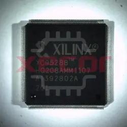
XC95288-15HQ208C
Programmable logic device with 48 macrocells
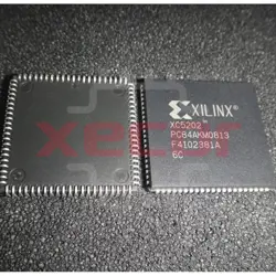
XC5202-6PC84C
This FPGA operates at a frequency of 83MHz and is designed using 0.5um technology
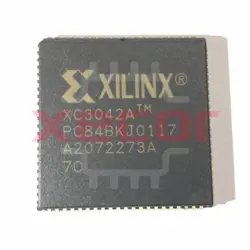
XC3042A-7PC84C
This product is a Programmable Logic IC that utilizes CMOS technology and features SMT for easy installation
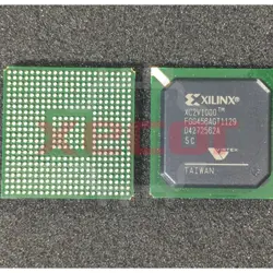
XC2V1000-5FGG456C
XC2V1000-5FGG456C Field Programmable Gate Array
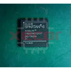
XC6SLX9-2CSG225C
FPGA with 715 CLBs and 667MHz
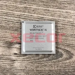
XC4VSX35-11FFG668I
XC4VSX35-11FFG668I, FCBGA-668 Programmable Logic Device