XC3S4000-4FGG900I
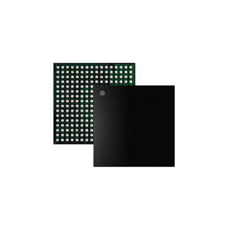
FPGA - Field Programmable Gate Array XC3S4000-4FGG900I
Inventory:9,757
- 90-day after-sales guarantee
- 365 Days Quality Guarantee
- Genuine Product Guarantee
- 7*24 hours service quarantee
-
Part Number : XC3S4000-4FGG900I
-
Package/Case : FBGA-900
-
Brands : Xilinx
-
Components Categories : FPGAs
-
Datesheet : XC3S4000-4FGG900I DataSheet (PDF)
The XC3S4000-4FGG900I is a high-performance FPGA (Field-Programmable Gate Array) from Xilinx.It features a large number of configurable logic blocks and programmable interconnects, making it suitable for a wide range of applications requiring custom digital logic implementations. (Note: The pin configuration below is a general representation. Refer to the specific datasheet for precise details.) Include a circuit diagram illustrating the connections and operation of the XC3S4000-4FGG900I FPGA for a visual representation. Note: For detailed technical specifications, please refer to the XC3S4000-4FGG900I datasheet. Functionality The XC3S4000-4FGG900I FPGA provides a platform for users to define their digital logic functions and create highly customized hardware solutions. It offers versatility and performance for a variety of applications. Usage Guide Q: Can the XC3S4000-4FGG900I be reprogrammed multiple times? Q: What is the maximum operating frequency supported by the XC3S4000-4FGG900I? For similar functionalities, consider these alternatives to the XC3S4000-4FGG900I:Overview of XC3S4000-4FGG900I
Pinout
Circuit Diagram
Key Features
Application
Frequently Asked Questions
A: Yes, the XC3S4000-4FGG900I is designed for reprogramming, allowing users to update the configuration as needed.
A: The XC3S4000-4FGG900I can operate at high clock frequencies, depending on the design constraints and setup.Equivalent
Specifications
The followings are basic parameters of the part selected concerning the characteristics of the part and categories it belongs to.
| Product Category | FPGA - Field Programmable Gate Array | RoHS | Details |
| Series | XC3S4000 | Number of Logic Elements | 62208 LE |
| Adaptive Logic Modules - ALMs | 27648 ALM | Embedded Memory | 1.69 Mbit |
| Number of I/Os | 633 I/O | Supply Voltage - Min | 1.14 V |
| Supply Voltage - Max | 1.26 V | Minimum Operating Temperature | - 40 C |
| Maximum Operating Temperature | + 100 C | Mounting Style | SMD/SMT |
| Package / Case | FBGA-900 | Brand | Xilinx |
| Distributed RAM | 432 kbit | Embedded Block RAM - EBR | 1728 kbit |
| Maximum Operating Frequency | 280 MHz | Moisture Sensitive | Yes |
| Number of Gates | 4000000 | Operating Supply Voltage | 1.2 V |
| Product Type | FPGA - Field Programmable Gate Array | Factory Pack Quantity | 1 |
| Subcategory | Programmable Logic ICs | Tradename | Spartan |
| Unit Weight | 2.779681 oz |
Warranty & Returns
Warranty, Returns, and Additional Information
-
QA & Return Policy
Parts Quality Guarantee: 365 days
Returns for refund: within 90 days
Returns for Exchange: within 90 days
-
Shipping and Package
Shipping:For example, FedEx, SF, UPS, or DHL.UPS, or DHL.
Parts Packaging Guarantee: Featuring 100% ESD anti-static protection, our packaging incorporates high toughness and superior buffering capabilities.
-
Payment
For example, channels like VISA, MasterCard, UnionPay, Western Union, PayPal, and more.
If you have specific payment channel preferences or requirements, please get in touch with our sales team for assistance.
Similar Product

AT91SAM7XC512-AU
ARM Microcontrollers - MCU LQFP IND TEMP

XC6SLX16-L1CSG225I
FPGA - Field Programmable Gate Array XC6SLX16-L1CSG225I

XC6SLX100T-3FGG484I
FPGA, SPARTAN-6, 296 I/O, FPBGA-484

SAF-XC161CJ-16F40F BB
16-bit Microcontrollers - MCU 16 BIT SNGL CHIP 5V 40MHz Flash

XC5VSX50T-1FFG665I
FPGA - Field Programmable Gate Array XC5VSX50T-1FFG665I

XC5VLX50T-1FFG665I
FPGA - Field Programmable Gate Array Connect to a released FG

XC5VLX85T-1FFG1136C
FPGA - Field Programmable Gate Array BOM fix route to Esperanza Green only Connect to Released FG

XC2S150-5PQG208I
Spartan®-II Field Programmable Gate Array (FPGA) IC 140 49152 3888 208-BFQFP

