
W972GG6JB25I
Winbond Electronics Corporation
Inventory:4,898
- 90-day after-sales guarantee
- 365 Days Quality Guarantee
- Genuine Product Guarantee
- 7*24 hours service quarantee
-
Part Number : W972GG6JB25I
-
Package/Case : BGA
-
Components Categories : Memory
-
Datesheet : W972GG6JB25I DataSheet (PDF)
Overview of W972GG6JB25I
SDRAM - DDR2 Memory IC 2Gbit Parallel 200 MHz 57.5 ns 84-WBGA (11x13)
Key Features
- Power Supply: VDD, VDDQ = 1.8 V ± 0.1 V
- Double Data Rate architecture: two data transfers per clock cycle
- CAS Latency: 3, 4, 5, 6 and 7
- Burst Length: 4 and 8
- Bi-directional, differential data strobes (DQS and DQS ) are transmitted / received with data
- Edge-aligned with Read data and center-aligned with Write data
- DLL aligns DQ and DQS transitions with clock
- Differential clock inputs (CLK and CLK )
- Data masks (DM) for write data
- Commands entered on each positive CLK edge, data and data mask are referenced to both edges of DQS
- Posted CAS programmable additive latency supported to make command and data bus efficiency
- Read Latency = Additive Latency plus CAS Latency (RL = AL + CL)
- Off-Chip-Driver impedance adjustment (OCD) and On-Die-Termination (ODT) for better signal quality
- Auto-precharge operation for read and write bursts
- Auto Refresh and Self Refresh modes
- Precharged Power Down and Active Power Down
- Write Data Mask
- Write Latency = Read Latency - 1 (WL = RL - 1)
- Interface: SSTL_18
- Packaged in WBGA 84 Ball (11x13 mm2), using Lead free materials with RoHS compliant
Specifications
The followings are basic parameters of the part selected concerning the characteristics of the part and categories it belongs to.
| Rohs Code | Yes | Part Life Cycle Code | Obsolete |
| Ihs Manufacturer | WINBOND ELECTRONICS CORP | Package Description | TFBGA, BGA84,9X15,32 |
| Reach Compliance Code | compliant | ECCN Code | EAR99 |
| HTS Code | 8542.32.00.36 | Samacsys Manufacturer | Winbond |
| Access Mode | MULTI BANK PAGE BURST | Access Time-Max | 0.4 ns |
| Additional Feature | AUTO/SELF REFRESH | Clock Frequency-Max (fCLK) | 400 MHz |
| I/O Type | COMMON | Interleaved Burst Length | 4,8 |
| JESD-30 Code | R-PBGA-B84 | Length | 13 mm |
| Memory Density | 2147483648 bit | Memory IC Type | DDR2 DRAM |
| Memory Width | 16 | Number of Functions | 1 |
| Number of Ports | 1 | Number of Terminals | 84 |
| Number of Words | 134217728 words | Number of Words Code | 128000000 |
| Operating Mode | SYNCHRONOUS | Operating Temperature-Max | 95 °C |
| Operating Temperature-Min | -40 °C | Organization | 128MX16 |
| Output Characteristics | 3-STATE | Package Body Material | PLASTIC/EPOXY |
| Package Code | TFBGA | Package Equivalence Code | BGA84,9X15,32 |
| Package Shape | RECTANGULAR | Package Style | GRID ARRAY, THIN PROFILE, FINE PITCH |
| Peak Reflow Temperature (Cel) | NOT SPECIFIED | Power Supplies | 1.8 V |
| Qualification Status | Not Qualified | Refresh Cycles | 8192 |
| Seated Height-Max | 1.2 mm | Self Refresh | YES |
| Sequential Burst Length | 4,8 | Standby Current-Max | 0.012 A |
| Supply Current-Max | 0.25 mA | Supply Voltage-Max (Vsup) | 1.9 V |
| Supply Voltage-Min (Vsup) | 1.7 V | Supply Voltage-Nom (Vsup) | 1.8 V |
| Surface Mount | YES | Technology | CMOS |
| Temperature Grade | INDUSTRIAL | Terminal Form | BALL |
| Terminal Pitch | 0.8 mm | Terminal Position | BOTTOM |
| Time@Peak Reflow Temperature-Max (s) | NOT SPECIFIED | Width | 11 mm |
Warranty & Returns
Warranty, Returns, and Additional Information
-
QA & Return Policy
Parts Quality Guarantee: 365 days
Returns for refund: within 90 days
Returns for Exchange: within 90 days
-
Shipping and Package
Shipping:For example, FedEx, SF, UPS, or DHL.UPS, or DHL.
Parts Packaging Guarantee: Featuring 100% ESD anti-static protection, our packaging incorporates high toughness and superior buffering capabilities.
-
Payment
For example, channels like VISA, MasterCard, UnionPay, Western Union, PayPal, and more.
If you have specific payment channel preferences or requirements, please get in touch with our sales team for assistance.
Similar Product
W971GG6SB-25
DRAM Chip DDR2 SDRAM 1Gbit 64Mx16 1.8V 84-Pin WBGA
W9751G6KB-25
DRAM 512Mb DDR2-800, x16
W9825G6JB-6I
DRAM 256Mb SDR SDRAM x16, 166MHz, Ind Temp
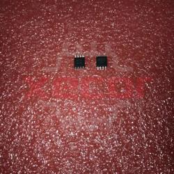
W25Q64FWSSIG
The W25Q64FWSSIG has a fast access time of 6ns and is housed in an 8-pin SOIC package
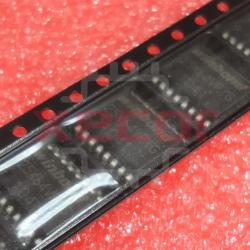
W25Q128FVSIG
IC chip for flash storage with a capacity of 128 megabits, featuring SPI and quad communication interfaces, housed in an 8SOIC package
W25X64VSFIG
8Mx8 Flash Memory
W25Q256FVEIG
NOR Flash Serial (SPI, Dual SPI, Quad SPI) 3V/3.3V 256M-bit 32M x 8 7ns 8-Pin WSON EP
W29N02GVSIAA
SLC NAND Flash Parallel 3V/3.3V 2G-bit 256M x 8 25ns Automotive 48-Pin TSOP-I