
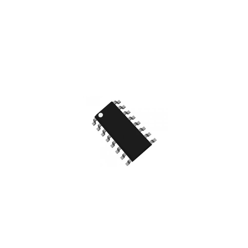
UCC5350MCD
Driver 10A 1-OUT Inv/Non-Inv 8-Pin SOIC Tube
Inventory:9,054
- 90-day after-sales guarantee
- 365 Days Quality Guarantee
- Genuine Product Guarantee
- 7*24 hours service quarantee
-
Part Number : UCC5350MCD
-
Package/Case : SOIC-8
-
Brands : Texas Instruments
-
Components Categories : Galvanically Isolated Gate Drivers
-
Datesheet : UCC5350MCD DataSheet (PDF)
Overview of UCC5350MCD
The UCC53x0 is a family of single-channel, isolated gate drivers designed to drive MOSFETs, IGBTs, SiC MOSFETs, and GaN FETs (UCC5350SBD). The UCC53x0S provides a split output that controls the rise and fall times individually. The UCC53x0M connects the gate of the transistor to an internal clamp to prevent false turnon caused by Miller current. The UCC53x0E has its UVLO2 referenced to GND2 to get a true UVLO reading.
The UCC53x0 is available in a 4 mm SOIC-8 (D) or 8.5 mm SOIC-8 (DWV) package and can support isolation voltage up to 3 kVRMS and 5 kVRMS respectively. With these various options the UCC53x0 family is a good fit for motor drives and industrial power supplies.
Compared to an optocoupler, the UCC53x0 family has lower part-to-part skew, lower propagation delay, higher operating temperature, and higher CMTI.
Key Features
- Feature Options
- Split Outputs (UCC53x0S)
- UVLO Referenced to GND2 (UCC53x0E)
- Miller Clamp Option (UCC53x0M)
- 8-pin D (4-mm Creepage) and
DWV (8.5mm Creepage) Package - 60-ns (Typical) Propagation Delay
- 100-kV/µs Minimum CMTI
- Isolation Barrier Life > 40 Years
- 3-V to 15-V Input Supply Voltage
- Up to 33-V Driver Supply Voltage
- 8-V and 12-V UVLO Options
- Negative 5-V Handling Capability on Input Pins
- Safety-Related Certifications:
- 7000-VPK Isolation DWV (Planned) and 4242-VPK Isolation D per DIN V VDE V 0884-11:2017-01 and DIN EN 61010-1
- 5000-VRMS DWV and 3000-VRMS D
Isolation Rating for 1 minute per UL 1577 - CQC Certification per GB4943.1-2011
D and DWV (Planned)
- CMOS Inputs
- Operating Temperature: –40°C to +125°C
Specifications
The followings are basic parameters of the part selected concerning the characteristics of the part and categories it belongs to.
| Number of channels | 1 | Isolation rating | Basic, Reinforced |
| Withstand isolation voltage (VISO) (Vrms) | 3000, 5000 | Working isolation voltage (VIOWM) (Vrms) | 990, 2121 |
| Transient isolation voltage (VIOTM) (VPK) | 4242, 7000 | Power switch | IGBT, MOSFET, SiCFET |
| Peak output current (A) | 10 | Features | Active miller clamp, Split output |
| Output VCC/VDD (max) (V) | 33 | Output VCC/VDD (min) (V) | 9.5 |
| Input VCC (min) (V) | 3 | Input VCC (max) (V) | 15 |
| Propagation delay time (µs) | 0.065 | Input threshold | CMOS |
| Operating temperature range (°C) | -40 to 125 | Rating | Catalog |
| Bus voltage (max) (V) | 2121 | Rise time (ns) | 10 |
| Fall time (ns) | 10 | Undervoltage lockout (typ) (V) | 8, 12 |
Warranty & Returns
Warranty, Returns, and Additional Information
-
QA & Return Policy
Parts Quality Guarantee: 365 days
Returns for refund: within 90 days
Returns for Exchange: within 90 days
-
Shipping and Package
Shipping:For example, FedEx, SF, UPS, or DHL.UPS, or DHL.
Parts Packaging Guarantee: Featuring 100% ESD anti-static protection, our packaging incorporates high toughness and superior buffering capabilities.
-
Payment
For example, channels like VISA, MasterCard, UnionPay, Western Union, PayPal, and more.
If you have specific payment channel preferences or requirements, please get in touch with our sales team for assistance.
Similar Product
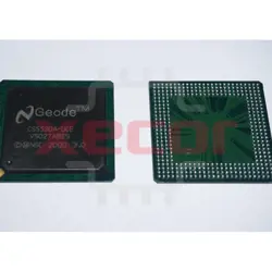
CS5530A-UCE
GEODE COMPANION DEVICE
FAN48685UC08X
Small form factor and low profile design
S32G274AABK0VUCT
Microprocessor S32G274AABK0VUCT with Arm Cortex-M7 and -A53 Cores
SII9587CNUC
Video ICs 4x HDMI 1.4 Port Processor with InstaPort, ARC, 3D, & MHL (225MHz)
SII9573CTUC
Video ICs 6 input 2 output HDMI v1.4 port processor, with InstaPort, InstaPrevue, MHL, ARC, 3D, OSD (300 MHz)
FPF1203LUCX
Power Switch Hi Side 1-OUT 2.2A 0.185Ohm 4-Pin WLCSP T/R
PUCC21750QDWRQ1
Automotive ±10-A, 5.7-kV RMS single channel isolated gate driver for SiC/IGBT with adv. protection 16-SOIC -40 to 125
UCC5350MCQDWVRQ1
Galvanically Isolated Gate Drivers 5-A/5-A, 3-k/5-kVRMS automotive single-channel isolated gate driver with Miller clamp 8-SOIC -40 to 125