
UCC27532DBVR
Driver 5A 2-OUT High and Low Side Non-Inv 6-Pin SOT-23 T/R
| Quantity | Unit Price(USD) | Ext. Price |
|---|---|---|
| 1 | $0.940 | $0.94 |
| 10 | $0.786 | $7.86 |
| 30 | $0.703 | $21.09 |
| 100 | $0.608 | $60.80 |
| 500 | $0.565 | $282.50 |
| 1000 | $0.547 | $547.00 |
Inventory:7,503
- 90-day after-sales guarantee
- 365 Days Quality Guarantee
- Genuine Product Guarantee
- 7*24 hours service quarantee
-
Part Number : UCC27532DBVR
-
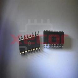
Package/Case : SOT-23-6
-
Brands : TI
-
Components Categories : Gate Drivers
-
Datesheet : UCC27532DBVR DataSheet (PDF)
Overview of UCC27532DBVR
The UCC27532 is a single-channel, high-speed, gate driver capable of effectively driving MOSFET and IGBT power switches by up to 2.5-A source and 5-A sink (asymmetrical drive) peak current. Strong sink capability in asymmetrical drive boosts immunity against parasitic Miller turn-on effect. The UCC27532 device also features a split-output configuration where the gate-drive current is sourced through OUTH pin and sunk through OUTL pin. This pin arrangement allows the user to apply independent turn-on and turn-off resistors to the OUTH and OUTL pins respectively and easily control the switching slew rates.
The driver has rail-to-rail drive capability and extremely small propagation delay typically 17 ns.
The UCC27532DBV has CMOS input threshold centered 55% rise and 45% fall in regards of VDD at VDD below or equal 18 V. When VDD is above 18 V, the input threshold remains fixed at its maximum level.
The driver has EN pin with fixed TTL compatible threshold. EN is internally pulled up; pulling EN low disables driver, while leaving it open provides normal operation. The EN pin can be used as an additional input with the same performance as the IN pin.
Leaving the input pin of driver open holds the output low. The logic behavior of the driver is shown in the application diagram, timing diagram and input and output logic truth table.
Internal circuitry on VDD pin provides an under voltage lockout function that holds output low until VDD supply voltage is within operating range.
The UCC27532 driver is offered in a 6-pin standard SOT-23 (DBV) package. The device operates over wide temperature range of 40°C to 140°C.
Key Features
- Low Cost Gate Driver (offering optimal solution for driving
FET and IGBTs) - Superior Replacement to Discrete Transistor Pair Drive (providing
easy interface with controller) - CMOS Compatible Input Logic Threshold (becomes fixed at VDD above 18 V)
- Split Outputs Allow Separate Turn-On and Turn-Off Tuning
- Enable with Fixed TTL Compatible Threshold
- High 2.5-A Source and 5-A Sink Peak Drive Currents at 18-V VDD
- Wide VDD Range From 10 V up to 35 V
- Input Pins Capable of Withstanding up to -5-V DC Below Ground
- Output Held Low When Inputs are Floating or During VDD UVLO
- Fast Propagation Delays (17-ns typical)
- Fast Rise and Fall Times
(15-ns and 7-ns typical with 1800-pF Load) - Under Voltage Lockout (UVLO)
- Used as a High-Side or Low-Side Driver (if designed with
proper bias and signal isolation) - Low Cost, Space Saving 6-Pin DBV (SOT-23) Package
- Operating Temperature Range of –40°C to 140°C
Specifications
The followings are basic parameters of the part selected concerning the characteristics of the part and categories it belongs to.
| Source Content uid | UCC27532DBVR | Pbfree Code | Yes |
| Rohs Code | Yes | Part Life Cycle Code | Active |
| Ihs Manufacturer | TEXAS INSTRUMENTS INC | Package Description | LSSOP, TSOP6,.11,37 |
| Reach Compliance Code | compliant | ECCN Code | EAR99 |
| HTS Code | 8542.39.00.01 | Samacsys Manufacturer | Texas Instruments |
| Interface IC Type | HALF BRIDGE BASED IGBT/MOSFET DRIVER | JESD-30 Code | R-PDSO-G6 |
| JESD-609 Code | e4 | Length | 2.9 mm |
| Moisture Sensitivity Level | 1 | Number of Channels | 1 |
| Number of Terminals | 6 | Operating Temperature-Max | 140 °C |
| Operating Temperature-Min | -40 °C | Output Current-Max | 5 A |
| Output Peak Current Limit-Nom | 5 A | Package Body Material | PLASTIC/EPOXY |
| Package Code | LSSOP | Package Equivalence Code | TSOP6,.11,37 |
| Package Shape | RECTANGULAR | Package Style | SMALL OUTLINE, LOW PROFILE, SHRINK PITCH |
| Peak Reflow Temperature (Cel) | 260 | Power Supplies | 18 V |
| Qualification Status | Not Qualified | Seated Height-Max | 1.45 mm |
| Supply Voltage-Nom | 18 V | Surface Mount | YES |
| Temperature Grade | AUTOMOTIVE | Terminal Finish | NICKEL PALLADIUM GOLD |
| Terminal Form | GULL WING | Terminal Pitch | 0.95 mm |
| Terminal Position | DUAL | Time@Peak Reflow Temperature-Max (s) | 30 |
| Width | 1.6 mm | Number of channels | 1 |
| Power switch | IGBT, MOSFET, SiCFET | Peak output current (A) | 5 |
| Input VCC (min) (V) | 10 | Input VCC (max) (V) | 32 |
| Features | Split Output | Operating temperature range (°C) | -40 to 140 |
| Rise time (ns) | 15 | Fall time (ns) | 7 |
| Propagation delay time (µs) | 0.017 | Input threshold | CMOS |
| Channel input logic | Non-Inverting, Single | Input negative voltage (V) | -5 |
| Rating | Catalog | Undervoltage lockout (typ) (V) | 8 |
| Driver configuration | Non-Inverting, Single |
Warranty & Returns
Warranty, Returns, and Additional Information
-
QA & Return Policy
Parts Quality Guarantee: 365 days
Returns for refund: within 90 days
Returns for Exchange: within 90 days
-
Shipping and Package
Shipping:For example, FedEx, SF, UPS, or DHL.UPS, or DHL.
Parts Packaging Guarantee: Featuring 100% ESD anti-static protection, our packaging incorporates high toughness and superior buffering capabilities.
-
Payment
For example, channels like VISA, MasterCard, UnionPay, Western Union, PayPal, and more.
If you have specific payment channel preferences or requirements, please get in touch with our sales team for assistance.
Similar Product
UCC28C43DR
The UCC28C43DR is a BiCMOS device designed for converting AC to DC with low power usage
UC28025DWR
Dual-use budget speed regulator
UCC27519DBVT
Driver for gate applications with high-speed and low-side functionality
UCC27712DR
Versatile interlock feature for added safety and control
UC3825N
AC-DC controllers and regulators, ROHS compliant
UC2825AN
Double ended UVLO
UC3854BN
95% duty cycle and frequency of 200 kHz
UCC2895N
High-frequency DIP-20 AC-DC Controllers & Regulators suitable for 10V~16.5V power supply inputs