
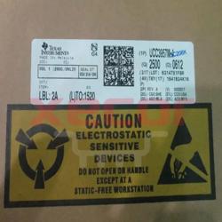
UCC27511AQDBVRQ1
Driver 8A 1-OUT Low Side Inv/Non-Inv Automotive AEC-Q100 6-Pin SOT-23 T/R
Inventory:3,432
- 90-day after-sales guarantee
- 365 Days Quality Guarantee
- Genuine Product Guarantee
- 7*24 hours service quarantee
-
Part Number : UCC27511AQDBVRQ1
-
Package/Case : SOT23-6
-
Brands : TI
-
Components Categories : Gate Drivers
-
Datesheet : UCC27511AQDBVRQ1 DataSheet (PDF)
Overview of UCC27511AQDBVRQ1
The UCC27511A-Q1 gate driver sets a new standard for reliability and performance in automotive gate driver solutions. Its robust design, fast switching speeds, and flexible configuration options make it a standout choice for applications where precision and efficiency are paramount. Whether driving MOSFETs, IGBTs, or GaN devices, this compact and powerful driver delivers consistent results, ensuring optimal operation in challenging environments. Upgrade your design with the UCC27511A-Q1 and experience the benefits of cutting-edge gate driver technology
Key Features
- Qualified for Automotive Applications
- AEC-Q100 Qualified With the Following Results:
- Device Temperature Grade 1: –40°C to 125°C
Ambient Operating Temperature Range - Device HBM ESD Classification Level 2
- Device CDM ESD Classification Level C4B
- Device Temperature Grade 1: –40°C to 125°C
- Low-Cost Gate-Driver Device Offering Superior
Replacement of NPN and PNP Discrete Solutions - 4-A Peak Source and 8-A Peak Sink Asymmetrical Drive
- Strong Sink Current Offers Enhanced Immunity Against
Miller Turnon - Split Output Configuration (Allows Easy and Independent
Adjustment of Turnon and Turnoff Speeds) in the
UCC27511A-Q1 - Fast Propagation Delays (13-ns typical)
- Fast Rise and Fall Times (9-ns and 7-ns typical)
- 4.5 to 18-V Single Supply Range
- Outputs Held Low During VDD UVLO (Ensures
Glitch-Free Operation at Power Up and Power Down) - TTL and CMOS Compatible Input-Logic Threshold
(Independent of Supply Voltage) - Hysteretic-Logic Thresholds for High-Noise Immunity
- Dual-Input Design (Choice of an Inverting (IN– Pin)
or Non-Inverting (IN+ Pin) Driver Configuration)- Unused Input Pin can be Used for Enable or
Disable Function
- Unused Input Pin can be Used for Enable or
- Output Held Low when Input Pins are Floating
- Input Pin Absolute Maximum Voltage Levels Not
Restricted by VDD Pin Bias Supply Voltage - Input Pins Capable of Withstanding –5-V DC Below
GND pin - Operating Temperature Range of –40°C to 140°C
- 6-Pin DBV (SOT-23) Package Option
Specifications
The followings are basic parameters of the part selected concerning the characteristics of the part and categories it belongs to.
| Number of channels | 1 | Power switch | GaNFET, IGBT, MOSFET |
| Peak output current (A) | 8 | Input VCC (min) (V) | 4.5 |
| Input VCC (max) (V) | 18 | Features | Split Output |
| Operating temperature range (°C) | -40 to 125 | Rise time (ns) | 9 |
| Fall time (ns) | 7 | Propagation delay time (µs) | 0.013 |
| Input threshold | CMOS, TTL | Channel input logic | Inverting, Non-Inverting |
| Input negative voltage (V) | -5 | Rating | Automotive |
| Undervoltage lockout (typ) (V) | 4 | Driver configuration | Inverting, Non-Inverting |
Warranty & Returns
Warranty, Returns, and Additional Information
-
QA & Return Policy
Parts Quality Guarantee: 365 days
Returns for refund: within 90 days
Returns for Exchange: within 90 days
-
Shipping and Package
Shipping:For example, FedEx, SF, UPS, or DHL.UPS, or DHL.
Parts Packaging Guarantee: Featuring 100% ESD anti-static protection, our packaging incorporates high toughness and superior buffering capabilities.
-
Payment
For example, channels like VISA, MasterCard, UnionPay, Western Union, PayPal, and more.
If you have specific payment channel preferences or requirements, please get in touch with our sales team for assistance.
Similar Product
UCC3957M-4
Battery Protection Li-Ion 25mA 4.35V 16-Pin SSOP Tube
UC28025DWR
Dual-use budget speed regulator
UCC27519DBVT
Driver for gate applications with high-speed and low-side functionality
UCC27712DR
Versatile interlock feature for added safety and control
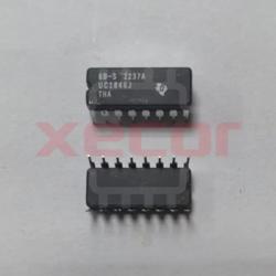
UC1846J
Texas Instruments UC1846J is a versatile 16-pin CDIP component
UC1844J
Current Mode PWM Controller 200mA 500kHz 8-Pin CDIP Tube
UC3825N
AC-DC controllers and regulators, ROHS compliant
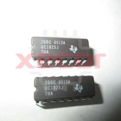
UC1825J
With its advanced features and robust design, this PWM controller ensures reliable performance in high-speed systems