
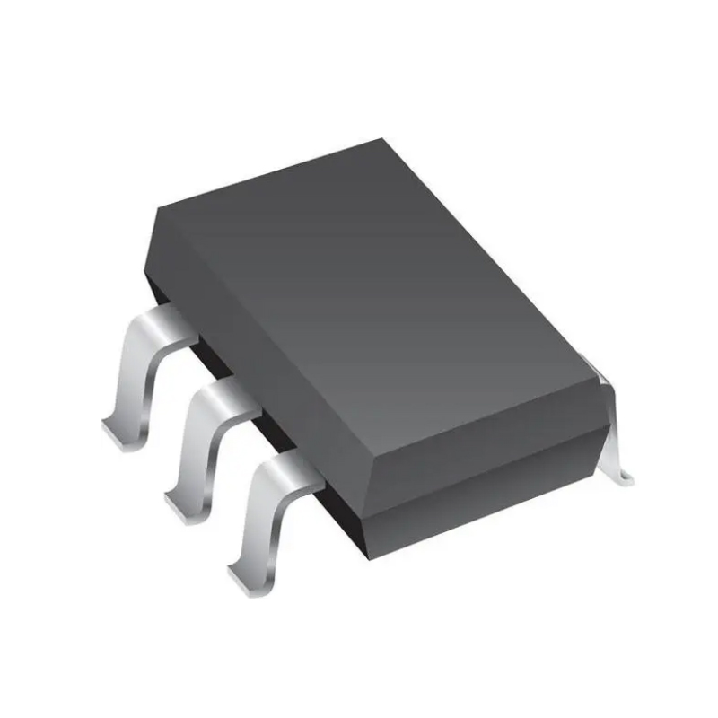
TSV911AIDBVR
Op Amp Single GP R-R I/O ±2.75V/5.5V 5-Pin SOT-23 T/R
| Quantity | Unit Price(USD) | Ext. Price |
|---|---|---|
| 1 | $0.465 | $0.46 |
| 10 | $0.374 | $3.74 |
| 30 | $0.335 | $10.05 |
| 100 | $0.285 | $28.50 |
| 500 | $0.264 | $132.00 |
| 1000 | $0.251 | $251.00 |
Inventory:5,756
- 90-day after-sales guarantee
- 365 Days Quality Guarantee
- Genuine Product Guarantee
- 7*24 hours service quarantee
-
Part Number : TSV911AIDBVR
-
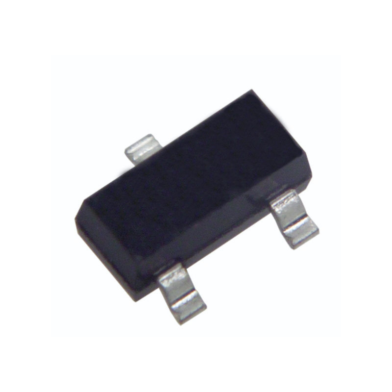
Package/Case : SOT23-5
-
Brands : TI
-
Components Categories : AmplifiersInstrumentation, OP Amps, Buffer Amps
-
Datesheet : TSV911AIDBVR DataSheet (PDF)
Overview of TSV911AIDBVR
The TSV91x family, which includes single-, dual-, and quad-channel operational amplifiers (op amps), is specifically designed for general-purpose applications. Featuring rail-to-rail input and output (RRIO) swings, wide bandwidth (8 MHz), and low offset voltage (0.3 mV, typical), this family is designed for a variety of applications that require a good balance between speed and power consumption. The op amps are unity-gain stable and feature an ultra-low input bias current, which enables the family to be used in applications with high-source impedances. The low input bias current allows the devices to be used for sensor interfaces, battery-supplied and portable applications, and active filtering.
The robust design of the TSV91x provides ease-of-use to the circuit designer. Features include a unity-gain stable, integrated RFI-EMI rejection filter, no phase reversal in overdrive condition, and high electrostatic discharge (ESD) protection (4-kV HBV).
Key Features
- Rail-to-rail input and output
- Low noise: 18 nV/√Hz at 1 kHz
- Low power consumption: 550 µA (typical)
- High-gain bandwidth: 8 MHz
- Operating supply voltage from 2.5 V to 5.5 V
- Low input bias current: 1 pA (typical)
- Low input offset voltage: 1.5 mV (maximum)
- Low offset voltage drift: ±0.5 µV/°C (typical)
- ESD internal protection: ±4-kV human-body model (HBM)
- Extended temperature range: –40°C to 125°C
Specifications
The followings are basic parameters of the part selected concerning the characteristics of the part and categories it belongs to.
| Number of channels | 1 | Total supply voltage (+5 V = 5, ±5 V = 10) (max) (V) | 5.5 |
| Total supply voltage (+5 V = 5, ±5 V = 10) (min) (V) | 2.5 | Rail-to-rail | In, Out |
| GBW (typ) (MHz) | 8 | Slew rate (typ) (V/µs) | 6.5 |
| Vos (offset voltage at 25°C) (max) (mV) | 1.5 | Iq per channel (typ) (mA) | 0.6 |
| Vn at 1 kHz (typ) (nV√Hz) | 18 | Rating | Catalog |
| Operating temperature range (°C) | -40 to 125 | Offset drift (typ) (µV/°C) | 0.53 |
| Features | EMI Hardened | CMRR (typ) (dB) | 103 |
| Iout (typ) (A) | 0.05 | Architecture | CMOS |
| Input common mode headroom (to negative supply) (typ) (V) | -0.5 | Input common mode headroom (to positive supply) (typ) (V) | 0.5 |
| Output swing headroom (to negative supply) (typ) (V) | 0.05 | Output swing headroom (to positive supply) (typ) (V) | -0.05 |
Warranty & Returns
Warranty, Returns, and Additional Information
-
QA & Return Policy
Parts Quality Guarantee: 365 days
Returns for refund: within 90 days
Returns for Exchange: within 90 days
-
Shipping and Package
Shipping:For example, FedEx, SF, UPS, or DHL.UPS, or DHL.
Parts Packaging Guarantee: Featuring 100% ESD anti-static protection, our packaging incorporates high toughness and superior buffering capabilities.
-
Payment
For example, channels like VISA, MasterCard, UnionPay, Western Union, PayPal, and more.
If you have specific payment channel preferences or requirements, please get in touch with our sales team for assistance.
Similar Product
LM4752TS
Audio Amp Speaker 2-CH Stereo 7W Class-AB 8-Pin(7+Tab) TO-263 Rail
LMH6321TS
Operational Amplifiers - Op Amps R 926-LMH6321TS/NOPB
TS3DV20812RHHR
Video Switch ICs 2-Gbps Differential Switch
TS321IDBVR
Texas Instruments TS321IDBVR Op Amp, 0.8MHz, 5 → 32 V, 5-Pin SOT-23
TSV911AIDCKR
Operational Amplifiers - Op Amps Single, 5.5-V, 8-MHz, RRIO operational amplifier 5-SC70 -40 to 125
TS321QDBVRQ1
Operational Amplifiers - Op Amps Auto Cat Lo-Pwr Sgl Op Amp
TPS3700DSER
WSON-6(1.5x1.5)
LM358LVIDR
5.5-V voltage range ideal for various circuit designs