
TPS70302PWPR
LDO Voltage Regulators 1A/2A Dual-Output
| Quantity | Unit Price(USD) | Ext. Price |
|---|---|---|
| 1 | $4.398 | $4.40 |
| 10 | $3.845 | $38.45 |
| 30 | $3.518 | $105.54 |
| 100 | $2.943 | $294.30 |
| 500 | $2.790 | $1,395.00 |
| 1000 | $2.721 | $2,721.00 |
Inventory:7,592
- 90-day after-sales guarantee
- 365 Days Quality Guarantee
- Genuine Product Guarantee
- 7*24 hours service quarantee
-
Part Number : TPS70302PWPR
-
Package/Case : HTSSOP-24
-
Brands : TI
-
Components Categories : Linear & low-dropout (LDO) regulators
-
Datesheet : TPS70302PWPR DataSheet (PDF)
Overview of TPS70302PWPR
The TPS703xx family of devices is designed to provide a complete power management solution for TI DSP, processor power, ASIC, FPGA, and digital applications where dual output voltage regulators are required. Easy programmability of the sequencing function makes this family ideal for any TI DSP application with power sequencing requirements. Differentiated features, such as accuracy, fast transient response, SVS supervisory circuit (power-on reset), manual reset inputs, and enable function, provide a complete system solution.
The TPS703xx family of voltage regulators offers very low dropout voltage and dual outputs with power up sequence control, designed primarily for DSP applications. These devices have low noise output performance without using any added filter bypass capacitors, and are designed to have a fast transient response and be stable with 47 µF low ESR capacitors.
These devices have fixed 3.3 V/2.5 V, 3.3 V/1.8 V, 3.3 V/1.5 V, 3.3 V/1.2 V, and adjustable voltage options. Regulator 1 can support up to 1 A, and regulator 2 can support up to 2 A. Separate voltage inputs allow the designer to configure the source power.
Because the PMOS pass element behaves as a low-value resistor, the dropout voltage is very low (typically 160mV on regulator 1) and is directly proportional to the output current. Additionally, since the PMOS pass element is a voltage-driven device, the quiescent current is very low and independent of output loading (maximum of 250 µA over the full range of output current). This LDO family also features a sleep mode; applying a high signal to EN (enable) shuts down both regulators, reducing the input current to 1 µA at TJ = +25°C.
The device is enabled when the EN pin is connected to a low-level input voltage. The output voltages of the two regulators are sensed at the VSENSE1 and VSENSE2 pins respectively.
The input signal at the SEQ pin controls the power-up sequence of the two regulators. When the device is enabled and the SEQ terminal is pulled high or left open, VOUT2 turns on first and VOUT1 remains off until VOUT2 reaches approximately 83% of its regulated output voltage. At that time VOUT1 is turned on. If VOUT2 is pulled below 83% (that is, in an overload condition) of its regulated voltage, VOUT1 is turned off. Pulling the SEQ terminal low reverses the power-up order and VOUT1 is turned on first. The SEQ pin is connected to an internal pull-up current source.
For each regulator, there is an internal discharge transistor to discharge the output capacitor when the regulator is turned off (disabled).
The PG1 pin reports the voltage condition at VOUT1. The PG1 pin can be used to implement an SVS (POR, or power-on reset) for the circuitry supplied by regulator 1.
The TPS703xx features a RESET (SVS, POR, or power-on reset). RESET is an active low, open drain output and requires a pull-up resistor for normal operation. When pulled up, RESET goes to a high impedance state (that is, logic high) after a 120 ms delay when all three of the following conditions are met. First, VIN1 must be above the undervoltage condition. Second, the manual reset (MR) pin must be in a high impedance state. Third, VOUT2 must be above approximately 95% of its regulated voltage. To monitor VOUT1, the PG1 output pin can be connected to MR1 or MR2. RESET can be used to drive power-on reset or a low-battery indicator. If RESET is not used, it can be left floating.
Internal bias voltages are powered by VIN1 and require 2.7V for full functionality. Each regulator input has an undervoltage lockout circuit that prevents each output from turning on until the respective input reaches 2.5 V.
Key Features
- Dual Output Voltages for Split-Supply Applications
- Independent Enable Functions (See Part Number TPS704xx
for Independent Enabling of Each Output) - Output Current Range of 1 A on Regulator 1 and 2A on Regulator 2
- Fast Transient Response
- Voltage Options: 3.3 V/2.5 V, 3.3 V/1.8 V, 3.3 V/1.5 V, 3.3 V/1.2 V,
and Dual Adjustable Outputs - Open Drain Power-On Reset with 120 ms Delay
- Open Drain Power Good for Regulator 1
- Ultralow 185 µA (typ) Quiescent Current
- 2 µA Input Current During Standby
- Low Noise: 78 µVRMS Without Bypass Capacitor
- Quick Output Capacitor Discharge Feature
- Two Manual Reset Inputs
- 2% Accuracy Over Load and Temperature
- Undervoltage Lockout (UVLO) Feature
- 24-Pin PowerPAD™ TSSOP Package
- Thermal Shutdown Protection
PowerPAD is a trademark of Texas Instruments.
All other trademarks are the property of their respective owners.
Specifications
The followings are basic parameters of the part selected concerning the characteristics of the part and categories it belongs to.
| Output options | Adjustable Output, Dual output, Fixed Output | Iout (max) (A) | 1 |
| Vin (max) (V) | 6 | Vin (min) (V) | 2.7 |
| Vout (max) (V) | 5.5 | Vout (min) (V) | 1.2 |
| Fixed output options (V) | 1.2, 1.5, 1.8, 2.5, 3.3 | Noise (µVrms) | 78 |
| Iq (typ) (mA) | 0.185 | Thermal resistance θJA (°C/W) | 30.9, 32 |
| Rating | Catalog | Load capacitance (min) (µF) | 22 |
| Regulated outputs (#) | 2 | Features | Enable, Output discharge, Power good, Sequencing and monitoring |
| Accuracy (%) | 2 | PSRR at 100 KHz (dB) | 22 |
| Dropout voltage (Vdo) (typ) (mV) | 160 | Operating temperature range (°C) | -40 to 125 |
Warranty & Returns
Warranty, Returns, and Additional Information
-
QA & Return Policy
Parts Quality Guarantee: 365 days
Returns for refund: within 90 days
Returns for Exchange: within 90 days
-
Shipping and Package
Shipping:For example, FedEx, SF, UPS, or DHL.UPS, or DHL.
Parts Packaging Guarantee: Featuring 100% ESD anti-static protection, our packaging incorporates high toughness and superior buffering capabilities.
-
Payment
For example, channels like VISA, MasterCard, UnionPay, Western Union, PayPal, and more.
If you have specific payment channel preferences or requirements, please get in touch with our sales team for assistance.
Similar Product
TPS74901RGWR
LDO Regulator Pos 0.798V to 3.6V 3A 20-Pin VQFN EP T/R
TPS3431SDRBR
Supervisory Circuits Standard programmable watchdog timer with enable 8-SON -40 to 125
TPS22965QWDSGTQ1
Power Switch Hi Side 1-OUT 4A 0.016Ohm Automotive AEC-Q100 8-Pin WSON EP T/R
TPS2511DGNR
Power Switch ICs - Power Distribution Charging Port Cntrlr & Crnt Ltd Pwr Sw
TPS3808G01QDRVRQ1
Processor Supervisor 0.405V 1 Active Low/Open Drain Automotive AEC-Q100 6-Pin WSON EP T/R
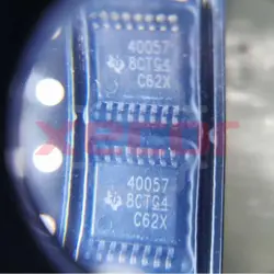
TPS40057PWPR
DC/DC Cntrlr Single-OUT Step Down 1000kHz 16-Pin HTSSOP EP T/R
TPS40170QRGYRQ1
DC/DC Cntrlr Single-OUT Step Down 20A 600kHz Automotive AEC-Q100 20-Pin VQFN EP T/R
TPS40200DR
DC/DC Cntrlr Single-OUT Step Down 3A 500kHz 8-Pin SOIC T/R