
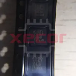
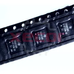
TPS60300DGS
Charge Pump STPUP 1.8V to 3.6V/3.3V 40mA/20mA 10-Pin VSSOP Tube
Inventory:5,073
- 90-day after-sales guarantee
- 365 Days Quality Guarantee
- Genuine Product Guarantee
- 7*24 hours service quarantee
-
Part Number : TPS60300DGS
-
Package/Case : VSSOP (DGS)-10
-
Brands : Texas Instruments
-
Components Categories : Voltage Regulators - DC DC Switching Regulators
-
Datesheet : TPS60300DGS DataSheet (PDF)
Overview of TPS60300DGS
The TPS6030x devices are a family of switched-voltage converters designed specifically for space-critical battery powered applications.
The TPS6030x step-up, regulated charge pumps generate a 3-V (±4%) or 3.3-V (±4%) output voltage from a 0.9-V to 1.8-V input voltage (one alkaline, NiCd, or NiMH battery).
Only five small 1-µF ceramic capacitors are required to build a complete high efficiency DC-DC charge pump converter. To achieve the high efficiency over a wide input voltage range, the charge pump automatically selects between a 3× or 4× conversion mode.
Output 1 (OUT1) can deliver a maximum of 40 mA from a 1-V input, with output 2 (OUT2) not loaded. OUT2 can deliver a maximum of 20 mA from a 1-V input, with OUT1 not loaded. Both outputs can be loaded at the same time, but the total output current of the first voltage doubler must not exceed 40 mA. For example, the load at output 1 is 20 mA and the load at output 2 is 10 mA.
The devices operate in the newly developed LinSkip mode. In this operating mode, the device switches seamlessly from the power saving, pulse-skip mode at light loads, to the low-noise, constant-frequency linear-regulation mode, when the output current exceeds the device-specific output current threshold.
A power-good function supervises the output voltage of OUT2 and can be used for power-up and power-down sequencing. Power good (PG) is offered as either open-drain or push-pull output.
Key Features
- Input Voltage Range From 0.9 V to 1.8 V
- Regulated 3-V or 3.3-V Output Voltage
- Up to 20-mA Output Current
- High Power Conversion Efficiency (up to 90%) Over a Wide Output Current Range, Optimized for 1.2-V Battery Voltage
- Additional Output With 2 Times VIN (OUT1)
- Device Quiescent Current Less Than 35 µA
- Supervisor Included; Open Drain or Push-Pull Power Good Output
- Minimum Number of External Components
- No Inductors Required
- Only Five Small, 1-µF Ceramic Capacitors Required
- Load Isolated From Battery During Shutdown
- Micro-Small 10-Pin MSOP (VSSOP) Package
All trademarks are the property of their respective owners.
Specifications
The followings are basic parameters of the part selected concerning the characteristics of the part and categories it belongs to.
| Vin (min) (V) | 0.9 | Vin (max) (V) | 1.8 |
| Vout (min) (V) | 3.3 | Vout (max) (V) | 3.3 |
| Iout (max) (A) | 0.04 | Regulated outputs (#) | 2 |
| Switching frequency (min) (kHz) | 470 | Switching frequency (max) (kHz) | 650 |
| Iq (typ) (mA) | 0.035 | Features | Enable, Power good |
| Operating temperature range (°C) | -40 to 85 | Rating | Catalog |
| Type | Charge pump |
Warranty & Returns
Warranty, Returns, and Additional Information
-
QA & Return Policy
Parts Quality Guarantee: 365 days
Returns for refund: within 90 days
Returns for Exchange: within 90 days
-
Shipping and Package
Shipping:For example, FedEx, SF, UPS, or DHL.UPS, or DHL.
Parts Packaging Guarantee: Featuring 100% ESD anti-static protection, our packaging incorporates high toughness and superior buffering capabilities.
-
Payment
For example, channels like VISA, MasterCard, UnionPay, Western Union, PayPal, and more.
If you have specific payment channel preferences or requirements, please get in touch with our sales team for assistance.
Similar Product
MAX31865ATP+T
Total solution offering a digital temperature reading from an RTD, including fault detection and input voltage protection
MAX31865ATP+
Specialized converter for RTD to digital conversion
TPS54291PWPR
Switching Voltage Regulators 4.5-18V Dual Sync Step Down Converter
TPS7A4001DGNT
Low-IQ 50-mA LDO voltage regulator capable of a 100-V output
TPS62120DCNT
Conv DC-DC 2V to 15V Synchronous Step Down Single-Out 1.2V to 5.5V 0.075A 8-Pin SOT-23 T/R
TPS65986ABZQZR
Low Speed/Full Speed/High Speed/Super Speed USB Interface Device USB 2.0 3.3V T/R 96-Pin BGA MICROSTAR JUNIOR

BQ76PL455ATPFCRQ1
Battery Monitoring/Battery Balancer 5mA Automotive 80-Pin TQFP T/R
TPS65982ABZBHR
Low Speed/Full Speed/High Speed/Super Speed USB Type-C and USB PD Controller and Power Switch USB 2.0/USB 3.0/USB 3.1 3.3V T/R 96-Pin NFBGA