
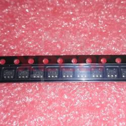
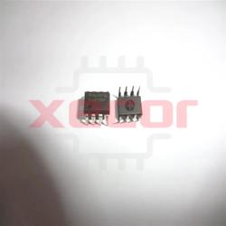
TLV9002IDR
This product operates with a wide supply voltage range of ±2.75V to 5.5V, making it versatile for different applications
| Quantity | Unit Price(USD) | Ext. Price |
|---|---|---|
| 5 | $0.206 | $1.03 |
| 50 | $0.169 | $8.45 |
| 150 | $0.153 | $22.95 |
| 500 | $0.133 | $66.50 |
| 2500 | $0.106 | $265.00 |
| 5000 | $0.100 | $500.00 |
Inventory:3,906
- 90-day after-sales guarantee
- 365 Days Quality Guarantee
- Genuine Product Guarantee
- 7*24 hours service quarantee
-
Part Number : TLV9002IDR
-
Package/Case : SOIC (D)-8
-
Brands : TI
-
Components Categories : AmplifiersInstrumentation, OP Amps, Buffer Amps
-
Datesheet : TLV9002IDR DataSheet (PDF)
The TLV9002IDR is a dual operational amplifier IC with rail-to-rail input and output capabilities, offering high precision and low noise performance. It is designed for various analog signal processing applications where accuracy and efficiency are essential. (Note: The pin configuration below is a general representation. Refer to the specific datasheet for precise details.) Include a circuit diagram illustrating the connections and operation of the TLV9002IDR IC for a visual representation. Note: For detailed technical specifications, please refer to the TLV9002IDR datasheet. Functionality The TLV9002IDR is a dual operational amplifier IC designed to amplify and process analog signals with high precision and low noise. It is a versatile component for various analog signal processing applications. Usage Guide Q: Is the TLV9002IDR suitable for low-power applications? Q: Can the TLV9002IDR operate with a single supply voltage? For similar functionalities, consider these alternatives to the TLV9002IDR:Overview of TLV9002IDR
Pinout
Circuit Diagram
Key Features
Application
Frequently Asked Questions
A: Yes, the TLV9002IDR operates efficiently at low supply voltages and is suitable for low-power analog signal processing applications.
A: Yes, the TLV9002IDR can operate with a single supply voltage ranging from +2.5V to +5.5V, making it versatile for various systems.Equivalent
Specifications
The followings are basic parameters of the part selected concerning the characteristics of the part and categories it belongs to.
| Number of channels | 2 | Total supply voltage (+5 V = 5, ±5 V = 10) (max) (V) | 5.5 |
| Total supply voltage (+5 V = 5, ±5 V = 10) (min) (V) | 1.8 | Rail-to-rail | In, Out |
| GBW (typ) (MHz) | 1 | Slew rate (typ) (V/µs) | 2 |
| Vos (offset voltage at 25°C) (max) (mV) | 1.5 | Iq per channel (typ) (mA) | 0.06 |
| Vn at 1 kHz (typ) (nV√Hz) | 30 | Rating | Catalog |
| Operating temperature range (°C) | -40 to 125 | Offset drift (typ) (µV/°C) | 0.6 |
| Features | Cost Optimized, EMI Hardened, Shutdown, Small Size | CMRR (typ) (dB) | 90 |
| Iout (typ) (A) | 0.04 | Architecture | CMOS |
| Input common mode headroom (to negative supply) (typ) (V) | -0.1 | Input common mode headroom (to positive supply) (typ) (V) | 0.1 |
| Output swing headroom (to negative supply) (typ) (V) | 0.01 | Output swing headroom (to positive supply) (typ) (V) | -0.01 |
Warranty & Returns
Warranty, Returns, and Additional Information
-
QA & Return Policy
Parts Quality Guarantee: 365 days
Returns for refund: within 90 days
Returns for Exchange: within 90 days
-
Shipping and Package
Shipping:For example, FedEx, SF, UPS, or DHL.UPS, or DHL.
Parts Packaging Guarantee: Featuring 100% ESD anti-static protection, our packaging incorporates high toughness and superior buffering capabilities.
-
Payment
For example, channels like VISA, MasterCard, UnionPay, Western Union, PayPal, and more.
If you have specific payment channel preferences or requirements, please get in touch with our sales team for assistance.
Similar Product
TL331IDBVR
Established French Electronics Distributor since 1988
TLC3702IDR
Push-pull output voltage comparator with dual functionality
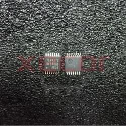
TLV4172IPWR
10MHzQuad10pATSSOP-1410OperationAmplifierROHS
TLC274CN
This device offers exceptional accuracy and stability, making it ideal for applications that demand reliable signal amplification
TLC272CP
Precision dual LiMCMOS amplifiers
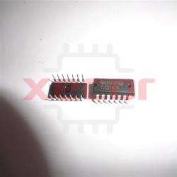
TL082CDR
Product TL082CDR is a dual JFET-input op amp with a 3-MHz bandwidth and a 13-V/μs slew rate
TL084IDR
The TL084IDR offers superior performance and reliability, making it ideal for precision measurement and control systems
TL072ACDR
Low noise amplifier