
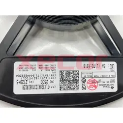
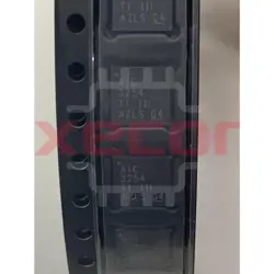
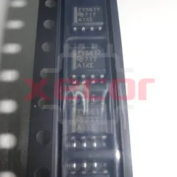
TLC5615CP
DAC 1-CH Resistor-String 10-bit 8-Pin PDIP Tube
| Quantity | Unit Price(USD) | Ext. Price |
|---|---|---|
| 1 | $3.703 | $3.70 |
| 10 | $3.276 | $32.76 |
| 50 | $3.024 | $151.20 |
| 100 | $2.715 | $271.50 |
| 500 | $2.596 | $1,298.00 |
| 1000 | $2.543 | $2,543.00 |
Inventory:9,502
- 90-day after-sales guarantee
- 365 Days Quality Guarantee
- Genuine Product Guarantee
- 7*24 hours service quarantee
-
Part Number : TLC5615CP
-
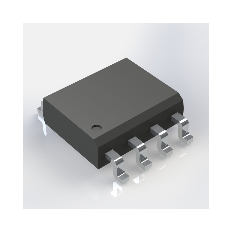
Package/Case : PDIP-8
-
Brands : TI
-
Components Categories : Precision DACs (≤10 MSPS)
-
Datesheet : TLC5615CP DataSheet (PDF)
Overview of TLC5615CP
The TLC5615 is a 10-bit voltage output digital-to-analog converter (DAC) with a buffered reference input (high impedance). The DAC has an output voltage range that is two times the reference voltage, and the DAC is monotonic. The device is simple to use, running from a single supply of 5V. A power-on-reset function is incorporated to ensure repeatable start-up conditions.
Digital control of the TLC5615 is over a three-wire serial bus that is CMOS compatible and easily interfaced to industry standard microprocessor and microcontroller devices. The device receives a 16-bit data word to produce the analog output. The digital inputs feature Schmitt triggers for high noise immunity. Digital communication protocols include the SPI™, QSPI™, and Microwire™ standards.
The 8-terminal small-outline D package allows digital control of analog functions in space-critical applications. The TLC5615C is characterized for operation from 0°C to +70°C. The TLC5615I is characterized for operation from -40°C to +85°C.
Key Features
- 10-Bit CMOS Voltage Output DAC in an 8-Terminal Package
- 5V Single Supply Operation
- 3-Wire Serial Interface
- High-Impedance Reference Inputs
- Voltage Output Range: 2 Times the Reference Input Voltage
- Internal Power-On Reset
- Low Power Consumption: 1.75mW Max
- Update Rate of 1.21MHz
- Settling Time to 0.5LSB: 12.5µs Typ
- Monotonic Over Temperature
- Pin-Compatible With the Maxim MAX515
- APPLICATIONS
- Battery-Powered Test Instruments
- Digital Offset and Gain Adjustment
- Battery Operated/Remote Industrial Controls
- Machine and Motion Control Devices
- Cellular Telephones
SPI, QSPI are trademarks of Motorola, Inc.
Microwire is a trademark of National Semiconductor Corporation.
All other trademarks are the property of their respective owners.
Specifications
The followings are basic parameters of the part selected concerning the characteristics of the part and categories it belongs to.
| Resolution (Bits) | 10 | Number of DAC channels | 1 |
| Interface type | SPI | Output type | Buffered Voltage |
| Settling time (µs) | 12.5 | Features | Low Power |
| Reference type | Ext | Architecture | String |
| Rating | Catalog | Output range (max) (mA/V) | 5.1 |
| Output range (min) (mA/V) | 0 | Sample/update rate (Msps) | 0.075 |
| Power consumption (typ) (mW) | 0.75 | Operating temperature range (°C) | -40 to 85, 0 to 70 |
Warranty & Returns
Warranty, Returns, and Additional Information
-
QA & Return Policy
Parts Quality Guarantee: 365 days
Returns for refund: within 90 days
Returns for Exchange: within 90 days
-
Shipping and Package
Shipping:For example, FedEx, SF, UPS, or DHL.UPS, or DHL.
Parts Packaging Guarantee: Featuring 100% ESD anti-static protection, our packaging incorporates high toughness and superior buffering capabilities.
-
Payment
For example, channels like VISA, MasterCard, UnionPay, Western Union, PayPal, and more.
If you have specific payment channel preferences or requirements, please get in touch with our sales team for assistance.
Similar Product
TLV320AIC3106IRGZR
General Purpose Audio Codec 2ADC / 2DAC Ch 48-Pin VQFN EP T/R
TLV320AIC3254IRHBR
General Purpose Audio Codec 2ADC / 2DAC Ch 32-Pin VQFN EP T/R
TLV5617AID
DAC 2-CH Resistor-String 10-bit 8-Pin SOIC Tube
TLC5615CD
1-Channel 10-Bit Digital-to-Analog Converter in SOIC Package
TLV320AIC3104IRHBR
CODEC with Low-Power Stereo Interface"
TLV2556MPWREP
EP 12B,200KSPS,11Ch Low Power
TLV320AIC1110PBS
Interface - CODECs Prog PCM w/Microphn Amps & Speaker Drvr
TLV320AIC14KIDBT
Interface - CODECs Low Power Mono Voice Codec