
TC7S32F
OR Gate 1-Element 2-IN CMOS 5-Pin SMV T/R
| Quantity | Unit Price(USD) | Ext. Price |
|---|---|---|
| 5 | $0.189 | $0.94 |
| 50 | $0.156 | $7.80 |
| 150 | $0.142 | $21.30 |
| 500 | $0.124 | $62.00 |
| 3000 | $0.113 | $339.00 |
| 6000 | $0.108 | $648.00 |
Inventory:6,840
- 90-day after-sales guarantee
- 365 Days Quality Guarantee
- Genuine Product Guarantee
- 7*24 hours service quarantee
-
Part Number : TC7S32F
-
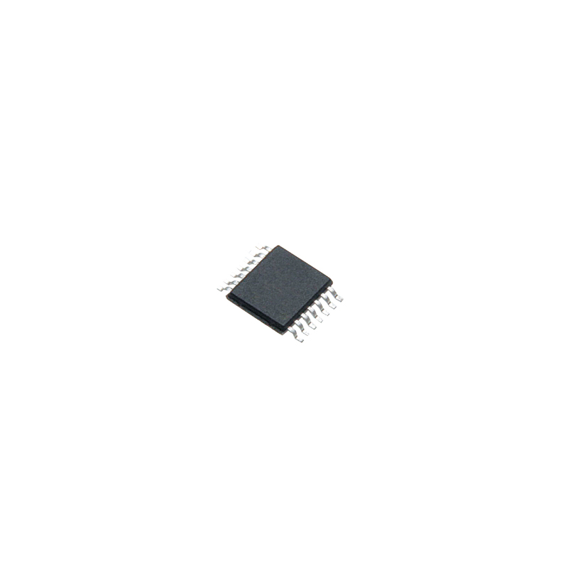
Package/Case : SSOP-5
-
Brands : TOSHIBA
-
Components Categories : Gates and Inverters
-
Datesheet : TC7S32F DataSheet (PDF)
The TC7S32F is a quad 2-input OR gate IC designed for digital logic applications. It combines four independent OR gates in a single package, allowing for versatile logic operations in electronic circuits. (Note: The pin configuration provided below is a general representation. Refer to the specific datasheet for precise details.) Include a circuit diagram illustrating the connections and operation of the TC7S32F IC for a visual representation. Note: For detailed technical specifications, please refer to the TC7S32F datasheet. Functionality The TC7S32F integrates four independent OR gates, enabling the implementation of various logical functions in electronic systems. It provides reliable logic operation for digital design applications. Usage Guide Q: Can the TC7S32F operate at higher frequencies? Q: Is the TC7S32F compatible with 5V logic levels? For similar functionalities, consider these alternatives to the TC7S32F:Overview of TC7S32F
Pinout
Circuit Diagram
Key Features
Application
Frequently Asked Questions
A: The TC7S32F is designed for standard logic applications and may not be suitable for very high-frequency operations. Consider alternative ICs for high-speed requirements.
A: Yes, the TC7S32F is compatible with standard 5V logic levels and can be easily interfaced with other digital components operating at 5V.Equivalent
Specifications
The followings are basic parameters of the part selected concerning the characteristics of the part and categories it belongs to.
| Source Content uid | TC7S32F | Rohs Code | Yes |
| Part Life Cycle Code | Obsolete | Ihs Manufacturer | TOSHIBA CORP |
| Part Package Code | SSOP | Package Description | LSSOP, TSOP5/6,.11,37 |
| Pin Count | 5 | Reach Compliance Code | |
| HTS Code | 8542.39.00.01 | Samacsys Manufacturer | Toshiba |
| Family | HC/UH | JESD-30 Code | R-PDSO-G5 |
| Length | 2.9 mm | Load Capacitance (CL) | 50 pF |
| Logic IC Type | OR GATE | Max I(ol) | 0.0026 A |
| Number of Functions | 1 | Number of Inputs | 2 |
| Number of Terminals | 5 | Operating Temperature-Max | 85 °C |
| Operating Temperature-Min | -40 °C | Package Body Material | PLASTIC/EPOXY |
| Package Code | LSSOP | Package Equivalence Code | SOP5,.11,37 |
| Package Shape | RECTANGULAR | Package Style | SMALL OUTLINE, LOW PROFILE, SHRINK PITCH |
| Peak Reflow Temperature (Cel) | NOT SPECIFIED | Power Supplies | 2/6 V |
| Propagation Delay (tpd) | 125 ns | Qualification Status | Not Qualified |
| Schmitt Trigger | NO | Seated Height-Max | 1.4 mm |
| Supply Voltage-Max (Vsup) | 6 V | Supply Voltage-Min (Vsup) | 2 V |
| Supply Voltage-Nom (Vsup) | 5 V | Surface Mount | YES |
| Technology | CMOS | Temperature Grade | INDUSTRIAL |
| Terminal Form | GULL WING | Terminal Pitch | 0.95 mm |
| Terminal Position | DUAL | Time@Peak Reflow Temperature-Max (s) | NOT SPECIFIED |
| Width | 1.6 mm |
Warranty & Returns
Warranty, Returns, and Additional Information
-
QA & Return Policy
Parts Quality Guarantee: 365 days
Returns for refund: within 90 days
Returns for Exchange: within 90 days
-
Shipping and Package
Shipping:For example, FedEx, SF, UPS, or DHL.UPS, or DHL.
Parts Packaging Guarantee: Featuring 100% ESD anti-static protection, our packaging incorporates high toughness and superior buffering capabilities.
-
Payment
For example, channels like VISA, MasterCard, UnionPay, Western Union, PayPal, and more.
If you have specific payment channel preferences or requirements, please get in touch with our sales team for assistance.
Similar Product

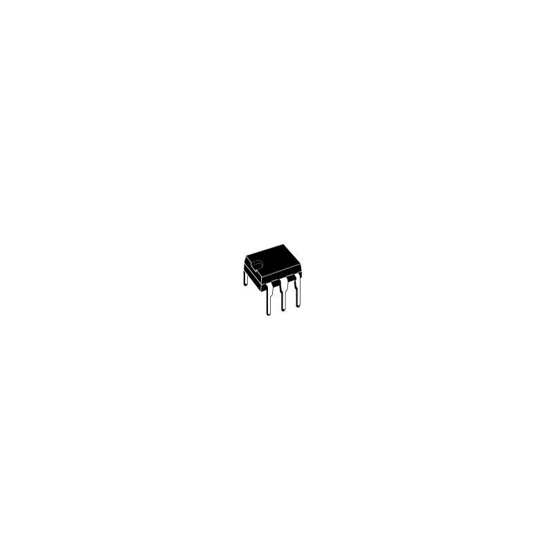
TC7S04FU
Six-pin logic circuit with inverter functionality and CMOS technology, housed in a plastic TSSOP package

TC7S08FU
PDSO5, 0.65 MM PITCH, PLASTIC

TC74HC14AF
CMOS Digital Integrated Circuit, Hex Schmitt Inverter, SOP14-P-300-1.27A
TC7SH02FU
Logic Circuit, 2-Input NOR, CMOS, 6 Pin, Plastic, TSSOP
TC4040BP
4000/14000/40000 Series
TC74VHC74FT
IC,Logic,74VHC Series TSSOP14,DUAL D-TY Toshiba TC74VHC74FT Dual D Type Flip Flop IC, 2 → 5.5 V, 14-Pin TSSOP
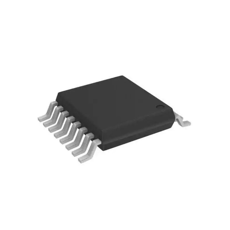
TC74VHC74F
Flip Flop D-Type Pos-Edge 2-Element 14-Pin SOP Tube
TC4094BP
Serial-to-Parallel Converter