
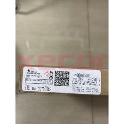
SN74LVC541APWR
Ideal for various electronic applications in need of signal buffering and line driving
| Quantity | Unit Price(USD) | Ext. Price |
|---|---|---|
| 5 | $0.251 | $1.26 |
| 50 | $0.203 | $10.15 |
| 150 | $0.183 | $27.45 |
| 500 | $0.156 | $78.00 |
| 2000 | $0.145 | $290.00 |
| 4000 | $0.138 | $552.00 |
Inventory:5,217
- 90-day after-sales guarantee
- 365 Days Quality Guarantee
- Genuine Product Guarantee
- 7*24 hours service quarantee
-
Part Number : SN74LVC541APWR
-
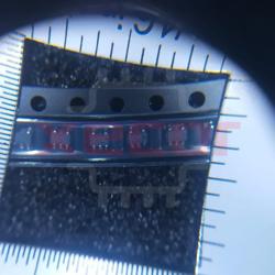
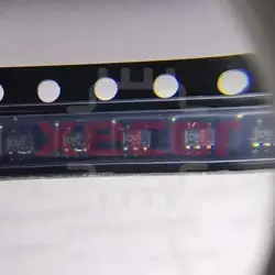
Package/Case : TSSOP (PW)-20
-
Brands : TI
-
Components Categories : Buffers, Drivers, Receivers, Transceivers
-
Datesheet : SN74LVC541APWR DataSheet (PDF)
The SN74LVC541APWR is an octal buffer and line driver IC designed for use in digital electronics applications. It features eight non-inverting buffers with 3-state outputs, making it suitable for driving bus lines or buffering signals in various digital systems. (Note: The pin configuration below is a general representation. Refer to the specific datasheet for precise details.) Include a circuit diagram illustrating the connections and operation of the SN74LVC541APWR IC for a visual representation. Note: For detailed technical specifications, please refer to the SN74LVC541APWR datasheet. Functionality The SN74LVC541APWR is an octal buffer and line driver IC that provides non-inverting buffers with 3-state outputs. It enables efficient signal buffering and driving of bus lines in digital systems. Usage Guide Q: What is the operating voltage range of the SN74LVC541APWR? Q: Can the SN74LVC541APWR be used for level shifting? For similar functionalities, consider these alternatives to the SN74LVC541APWR:Overview of SN74LVC541APWR
Pinout
Circuit Diagram
Key Features
Application
Frequently Asked Questions
A: The SN74LVC541APWR operates from 1.65V to 5.5V.
A: Yes, the SN74LVC541APWR can be used for level shifting applications where signals need to be translated between different voltage levels.Equivalent
Specifications
The followings are basic parameters of the part selected concerning the characteristics of the part and categories it belongs to.
| Technology family | LVC | Supply voltage (min) (V) | 1.65 |
| Supply voltage (max) (V) | 3.6 | Number of channels | 8 |
| IOL (max) (mA) | 24 | Supply current (max) (µA) | 10 |
| IOH (max) (mA) | -24 | Input type | Standard CMOS |
| Output type | 3-State | Features | Balanced outputs, Very high speed (tpd 5-10ns) |
| Rating | Catalog | Operating temperature range (°C) | -40 to 125 |
Warranty & Returns
Warranty, Returns, and Additional Information
-
QA & Return Policy
Parts Quality Guarantee: 365 days
Returns for refund: within 90 days
Returns for Exchange: within 90 days
-
Shipping and Package
Shipping:For example, FedEx, SF, UPS, or DHL.UPS, or DHL.
Parts Packaging Guarantee: Featuring 100% ESD anti-static protection, our packaging incorporates high toughness and superior buffering capabilities.
-
Payment
For example, channels like VISA, MasterCard, UnionPay, Western Union, PayPal, and more.
If you have specific payment channel preferences or requirements, please get in touch with our sales team for assistance.
Similar Product
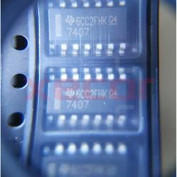
SN7407DR
High-voltage open-collector output configuration
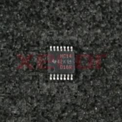
SN74HC14PWR
Inverter Schmitt Trigger 6-Element CMOS 14-Pin TSSOP T/R
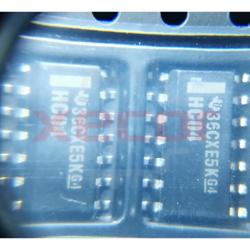
SN74HC04DR
Inverter 6-Element CMOS Automotive 14-Pin SOIC T/R
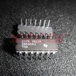
SN5404J
Contains 6 inverters with a voltage range of 4.5V to 5.5V
SN74AHC14PWR
Inverter Schmitt Trigger 6-Element CMOS 14-Pin TSSOP T/R
SN74LVC1G06DCKR
Buffer/Driver 1-CH Inverting Open Drain CMOS 5-Pin SC-70 T/R
SN74LVC1G32DCKR
Positive logic gates with dual inputs
SN74LVC1G126DCKR
Buffer/Line Driver 1-CH Non-Inverting 3-ST CMOS 5-Pin SC-70 T/R