
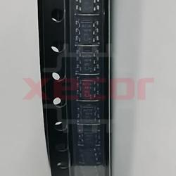
SN74AVC4T774PWR
Dual-supply operation for versatile applications
| Quantity | Unit Price(USD) | Ext. Price |
|---|---|---|
| 1 | $0.502 | $0.50 |
| 10 | $0.427 | $4.27 |
| 30 | $0.385 | $11.55 |
| 100 | $0.340 | $34.00 |
| 500 | $0.319 | $159.50 |
| 1000 | $0.309 | $309.00 |
Inventory:4,015
- 90-day after-sales guarantee
- 365 Days Quality Guarantee
- Genuine Product Guarantee
- 7*24 hours service quarantee
-
Part Number : SN74AVC4T774PWR
-
Package/Case : TSSOP (PW)-16
-
Brands : TI
-
Components Categories : Translators, Level Shifters
-
Datesheet : SN74AVC4T774PWR DataSheet (PDF)
The SN74AVC4T774PWR is a quadruple voltage level translator and buffer IC designed for bidirectional voltage translation between different logic levels. It features four independent translation channels, offering a versatile solution for interfacing between systems with different voltage requirements. (Note: The pin configuration below is a general representation. Refer to the specific datasheet for precise details.) Include a circuit diagram illustrating the connections and operation of the SN74AVC4T774PWR IC for a visual representation. Note: For detailed technical specifications, please refer to the SN74AVC4T774PWR datasheet. Functionality The SN74AVC4T774PWR is a versatile voltage level translator and buffer IC that facilitates seamless communication between systems with different voltage requirements. It ensures reliable signal integrity and compatibility in mixed-voltage environments. Usage Guide Q: Can the SN74AVC4T774PWR handle bidirectional voltage translation? Q: What is the operating frequency range of the SN74AVC4T774PWR? For similar functionalities, consider these alternatives to the SN74AVC4T774PWR:Overview of SN74AVC4T774PWR
Pinout
Circuit Diagram
Key Features
Application
Frequently Asked Questions
A: Yes, the SN74AVC4T774PWR is designed for bidirectional voltage translation between different logic levels in both directions.
A: The SN74AVC4T774PWR offers high-speed operation suitable for applications with frequency requirements up to several megahertz.Equivalent
Specifications
The followings are basic parameters of the part selected concerning the characteristics of the part and categories it belongs to.
| Technology family | AVC | Applications | JTAG, SPI, UART |
| Bits (#) | 4 | High input voltage (min) (V) | 0.78 |
| High input voltage (max) (V) | 3.6 | Vout (min) (V) | 1.2 |
| Vout (max) (V) | 3.6 | Data rate (max) (MBps) | 380 |
| IOH (max) (mA) | -12 | IOL (max) (mA) | 12 |
| Supply current (max) (µA) | 16 | Features | Output enable, Overvoltage tolerant inputs, Partial power down (Ioff) |
| Input type | Standard CMOS | Output type | Balanced CMOS, Push-Pull |
| Rating | Catalog | Operating temperature range (°C) | -40 to 85 |
Warranty & Returns
Warranty, Returns, and Additional Information
-
QA & Return Policy
Parts Quality Guarantee: 365 days
Returns for refund: within 90 days
Returns for Exchange: within 90 days
-
Shipping and Package
Shipping:For example, FedEx, SF, UPS, or DHL.UPS, or DHL.
Parts Packaging Guarantee: Featuring 100% ESD anti-static protection, our packaging incorporates high toughness and superior buffering capabilities.
-
Payment
For example, channels like VISA, MasterCard, UnionPay, Western Union, PayPal, and more.
If you have specific payment channel preferences or requirements, please get in touch with our sales team for assistance.
Similar Product
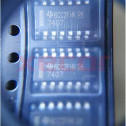
SN7407DR
High-voltage open-collector output configuration
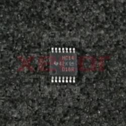
SN74HC14PWR
Inverter Schmitt Trigger 6-Element CMOS 14-Pin TSSOP T/R
SN74LVC1G126DCKR
Buffer/Line Driver 1-CH Non-Inverting 3-ST CMOS 5-Pin SC-70 T/R
SN74LVC1G126DBVR
Buffer/Line Driver 1-CH Non-Inverting 3-ST CMOS 5-Pin SOT-23 T/R
SN74LVC2G34DBVR
Buffer 2-CH Non-Inverting Push-Pull CMOS 6-Pin SOT-23 T/R

SN74AHC1G08DCKR
AND Gate 1-Element 2-IN CMOS 5-Pin SC-70 T/R

SN74LVC1G11DCKR
SN74LVC1G11DCKR Product Code
SN74AVC8T245RHLR
The SN74AVC8T245RHLR is an 8-bit bus transceiver with configurable voltage-level shifting and 3-state outputs in a 24-VQFN package