
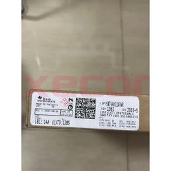
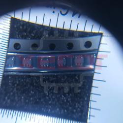
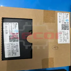
SN74ALVC164245DGGR
Voltage Level Translator 16-CH Bidirectional 48-Pin TSSOP T/R
| Quantity | Unit Price(USD) | Ext. Price |
|---|---|---|
| 1 | $1.688 | $1.69 |
| 10 | $1.461 | $14.61 |
| 30 | $1.335 | $40.05 |
| 100 | $1.196 | $119.60 |
| 500 | $1.051 | $525.50 |
| 1000 | $1.024 | $1,024.00 |
Inventory:8,234
- 90-day after-sales guarantee
- 365 Days Quality Guarantee
- Genuine Product Guarantee
- 7*24 hours service quarantee
-
Part Number : SN74ALVC164245DGGR
-
Package/Case : TSSOP (DGG)-48
-
Brands : TI
-
Components Categories : Translators, Level Shifters
-
Datesheet : SN74ALVC164245DGGR DataSheet (PDF)
Overview of SN74ALVC164245DGGR
This 16-bit (dual-octal) noninverting bus transceiver contains two separate supply rails. B port has VCCB, which is set to operate at 3.3 V and 5 V. A port has VCCA, which is set to operate at 2.5 V and 3.3 V. This allows for translation from a 2.5-V to a 3.3-V environment, and vice versa, or from a 3.3-V to a 5-V environment, and vice versa.
The SN74ALVC164245 is designed for asynchronous communication between data buses. The control circuitry (1DIR, 2DIR, 1OE, and 2OE) is powered by VCCA.
To ensure the high-impedance state during power up or power down, the output-enable (OE) input should be tied to VCC through a pullup resistor; the minimum value of the resistor is determined by the current-sinking capability of the driver.
The logic levels of the direction-control (DIR) input and the output-enable (OE) input activate either the B-port outputs or the A-port outputs or place both output ports into the high-impedance mode. The device transmits data from the A bus to the B bus when the B-port outputs are activated, and from the B bus to the A bus when the A-port outputs are activated. The input circuitry on both A and B ports always is active and must have a logic HIGH or LOW level applied to prevent excess ICC and ICCZ.
Key Features
- Member of the Texas Instruments Widebus™ Family
- Maximum tpd of 5.8 ns at 3.3 V
- ±24-mA Output Drive at 3.3 V
- Control Inputs VIH/VIL Levels Are Referenced to VCCA Voltage
- Latch-Up Performance Exceeds 250 mA Per JESD 17
- APPLICATIONS
- Electronic Points of Sale
- Printers and Other Peripherals
- Motor Drives
- Wireless and Telecom Infrastructures
- Wearable Health and Fitness Devices
All other trademarks are the property of their respective owners
Specifications
The followings are basic parameters of the part selected concerning the characteristics of the part and categories it belongs to.
| Technology family | ALVC | Bits (#) | 16 |
| High input voltage (min) (V) | 1.7 | High input voltage (max) (V) | 5.5 |
| Vout (min) (V) | 2.3 | Vout (max) (V) | 5.5 |
| Data rate (max) (MBps) | 300 | IOH (max) (mA) | -24 |
| IOL (max) (mA) | 24 | Supply current (max) (µA) | 40 |
| Features | Output enable | Input type | Standard CMOS |
| Output type | 3-State, Balanced CMOS, Push-Pull | Rating | Catalog |
| Operating temperature range (°C) | -40 to 85 |
Warranty & Returns
Warranty, Returns, and Additional Information
-
QA & Return Policy
Parts Quality Guarantee: 365 days
Returns for refund: within 90 days
Returns for Exchange: within 90 days
-
Shipping and Package
Shipping:For example, FedEx, SF, UPS, or DHL.UPS, or DHL.
Parts Packaging Guarantee: Featuring 100% ESD anti-static protection, our packaging incorporates high toughness and superior buffering capabilities.
-
Payment
For example, channels like VISA, MasterCard, UnionPay, Western Union, PayPal, and more.
If you have specific payment channel preferences or requirements, please get in touch with our sales team for assistance.
Similar Product

SN74154N
4-to-16 Decoder
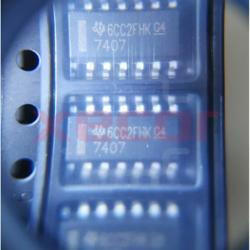
SN7407DR
High-voltage open-collector output configuration
SN74HC14PWR
Inverter Schmitt Trigger 6-Element CMOS 14-Pin TSSOP T/R
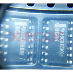
SN74HC04DR
Inverter 6-Element CMOS Automotive 14-Pin SOIC T/R
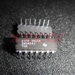
SN5404J
Contains 6 inverters with a voltage range of 4.5V to 5.5V
SN74AHC14PWR
Inverter Schmitt Trigger 6-Element CMOS 14-Pin TSSOP T/R
SN74LVC1G06DCKR
Buffer/Driver 1-CH Inverting Open Drain CMOS 5-Pin SC-70 T/R
SN74LVC1G32DCKR
Positive logic gates with dual inputs