
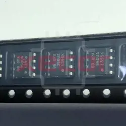
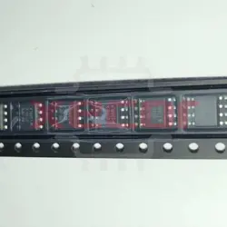
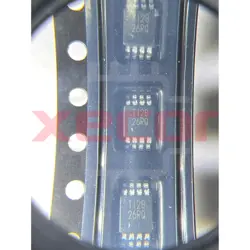
OPA657U
Op Amp Single High Speed Amplifier ±6V/12V 8-Pin SOIC Tube
Inventory:8,090
- 90-day after-sales guarantee
- 365 Days Quality Guarantee
- Genuine Product Guarantee
- 7*24 hours service quarantee
-
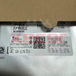
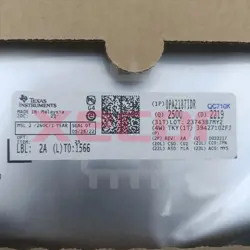
Part Number : OPA657U
-
Package/Case : SOIC-8
-
Brands : TI
-
Components Categories : High-speed op amps (GBW ≥ 50 MHz)
-
Datesheet : OPA657U DataSheet (PDF)
Overview of OPA657U
The OPA657 device combines a high-gain bandwidth, low-distortion, voltage-feedback operational amplifier with a low-voltage noise JFET-input stage to offer a very high dynamic range amplifier for high-precision ADC (analog-to-digital converter) driving or wideband transimpedance applications. Photodiode applications see improved noise and bandwidth using this decompensated, high-gain bandwidth amplifier.
Very low level signals can be significantly amplified in a single OPA657 gain stage with exceptional bandwidth and accuracy. Having a high 1.6-GHz gain bandwidth product gives greater than 10-MHz signal bandwidths up to gains of 160 V/V (44 dB). The very low input bias current and capacitance supports this performance even for relatively high source impedances.
Broadband photodetector applications benefit from the low-voltage noise JFET inputs for the OPA657. The JFET input contributes virtually no current noise while for broadband applications, a low voltage noise is also required. The low 4.8 nV/√Hz input voltage noise provides exceptional input sensitivity for higher bandwidth applications. The example shown below gives a total equivalent input noise current of 1.8 pA/√Hz over a 10-MHz bandwidth.
Key Features
- High Gain Bandwidth Product: 1.6 GHz
- High Bandwidth 275 MHz (G = 10)
- Slew Rate 700 V/µs (G = 10, 1-V Step)
- Available in High Grade With Improved DC
Specifications - Operating Temperature Range: –40°C to 85°C
- Low-Input Offset Voltage: ±250 µV
- Low-Input Bias Current: 2 pA
- Low-Input Voltage Noise: 4.8 nV/√Hz
- High-Output Current: 70 mA
- Fast Overdrive Recovery
Specifications
The followings are basic parameters of the part selected concerning the characteristics of the part and categories it belongs to.
| Architecture | FET / CMOS Input, Voltage FB | Number of channels | 1 |
| Total supply voltage (+5 V = 5, ±5 V = 10) (min) (V) | 8 | Total supply voltage (+5 V = 5, ±5 V = 10) (max) (V) | 12 |
| GBW (typ) (MHz) | 1600 | BW at Acl (MHz) | 350 |
| Acl, min spec gain (V/V) | 7 | Slew rate (typ) (V/µs) | 700 |
| Vn at flatband (typ) (nV√Hz) | 4.8 | Vn at 1 kHz (typ) (nV√Hz) | 7 |
| Iq per channel (typ) (mA) | 14 | Vos (offset voltage at 25°C) (max) (mV) | 1.8 |
| Rail-to-rail | No | Features | Decompensated |
| Rating | Catalog | Operating temperature range (°C) | -40 to 85 |
| CMRR (typ) (dB) | 89 | Input bias current (max) (pA) | 20 |
| Offset drift (typ) (µV/°C) | 2 | Iout (typ) (mA) | 70 |
| 2nd harmonic (dBc) | 74 | 3rd harmonic (dBc) | 106 |
| Frequency of harmonic distortion measurement (MHz) | 5 |
Warranty & Returns
Warranty, Returns, and Additional Information
-
QA & Return Policy
Parts Quality Guarantee: 365 days
Returns for refund: within 90 days
Returns for Exchange: within 90 days
-
Shipping and Package
Shipping:For example, FedEx, SF, UPS, or DHL.UPS, or DHL.
Parts Packaging Guarantee: Featuring 100% ESD anti-static protection, our packaging incorporates high toughness and superior buffering capabilities.
-
Payment
For example, channels like VISA, MasterCard, UnionPay, Western Union, PayPal, and more.
If you have specific payment channel preferences or requirements, please get in touch with our sales team for assistance.
Similar Product
OPA350UA
rail-to-rail single operational amplifier for single-supply applications
OPA227U
With advanced technology and superior design, the OPA227U delivers unmatched accuracy and minimal background noise
OPA1632DGN
channel audio amplifier IC OPA1632DGN in HVSSOP8 package supports power supply voltages between 5VDC and 30VDC
OPA2209AIDGKT
Dual Operational Amplifier with Low Noise Performance and Rail-to-Rail Output Capability at ±18V/36V
OPA2277U/2K5
1MHz Bandwidth Operational Amplifier General Purpose in 8-SOIC IC
OPA2182IDGKR
Operational Amplifiers - Op Amps Industry’s lowest offset drift (0.012 uV/°C, max), 5.7 nV/rtHz, MUX-friendly 36V op amp 8-VSSOP -40 to 125
OPA2192IDR
Op Amp Dual Precision Amplifier R-R I/O ±18V/36V 8-Pin SOIC T/R
OPA2187IDR
Operational Amplifiers - Op Amps 1AuV Vos, 0.005AuV/A C Low-Power 36V