
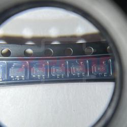
OPA365AIDBVR
Op Amp Single High Speed Amplifier R-R I/O ±2.75V/5.5V 5-Pin SOT-23 T/R
| Quantity | Unit Price(USD) | Ext. Price |
|---|---|---|
| 1 | $0.886 | $0.89 |
| 10 | $0.742 | $7.42 |
| 30 | $0.663 | $19.89 |
| 100 | $0.573 | $57.30 |
| 500 | $0.535 | $267.50 |
| 1000 | $0.516 | $516.00 |
Inventory:7,589
- 90-day after-sales guarantee
- 365 Days Quality Guarantee
- Genuine Product Guarantee
- 7*24 hours service quarantee
-
Part Number : OPA365AIDBVR
-
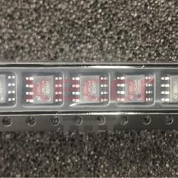
Package/Case : SOT23-5
-
Brands : TI
-
Components Categories : AmplifiersInstrumentation, OP Amps, Buffer Amps
-
Datesheet : OPA365AIDBVR DataSheet (PDF)
The OPA365AIDBVR is a precision operational amplifier with low offset voltage and low noise, ideal for precision signal conditioning applications. It offers high precision and performance, making it suitable for various analog signal processing tasks. (Note: The pin configuration below is a general representation. Refer to the specific datasheet for precise details.) Include a circuit diagram illustrating the connections and operation of the OPA365AIDBVR IC for a visual representation. Note: For detailed technical specifications, please refer to the OPA365AIDBVR datasheet. Functionality The OPA365AIDBVR is designed to provide precise amplification and signal conditioning for analog signals. It ensures accurate processing of signals in various applications that demand high precision. Usage Guide Q: Is the OPA365AIDBVR suitable for high-precision audio applications? Q: What is the operating voltage range of the OPA365AIDBVR? For similar functionalities, consider these alternatives to the OPA365AIDBVR:Overview of OPA365AIDBVR
Pinout
Circuit Diagram
Key Features
Application
Frequently Asked Questions
A: Yes, the OPA365AIDBVR's precision and low noise make it suitable for high-fidelity audio applications where accuracy is crucial.
A: The OPA365AIDBVR can operate within a wide voltage range typically from ±2.25V to ±18V.Equivalent
Specifications
The followings are basic parameters of the part selected concerning the characteristics of the part and categories it belongs to.
| Architecture | FET / CMOS Input, Voltage FB | Number of channels | 1 |
| Total supply voltage (+5 V = 5, ±5 V = 10) (min) (V) | 2.2 | Total supply voltage (+5 V = 5, ±5 V = 10) (max) (V) | 5.5 |
| GBW (typ) (MHz) | 50 | BW at Acl (MHz) | 50 |
| Acl, min spec gain (V/V) | 1 | Slew rate (typ) (V/µs) | 25 |
| Vn at flatband (typ) (nV√Hz) | 4.5 | Vn at 1 kHz (typ) (nV√Hz) | 4.5 |
| Iq per channel (typ) (mA) | 4.6 | Vos (offset voltage at 25°C) (max) (mV) | 0.2 |
| Rail-to-rail | In, Out | Features | Zero Crossover |
| Rating | Catalog | Operating temperature range (°C) | -40 to 125 |
| CMRR (typ) (dB) | 120 | Input bias current (max) (pA) | 10 |
| Offset drift (typ) (µV/°C) | 1 | Iout (typ) (mA) | 65 |
| 2nd harmonic (dBc) | 81 | 3rd harmonic (dBc) | 93 |
| Frequency of harmonic distortion measurement (MHz) | 1 |
Warranty & Returns
Warranty, Returns, and Additional Information
-
QA & Return Policy
Parts Quality Guarantee: 365 days
Returns for refund: within 90 days
Returns for Exchange: within 90 days
-
Shipping and Package
Shipping:For example, FedEx, SF, UPS, or DHL.UPS, or DHL.
Parts Packaging Guarantee: Featuring 100% ESD anti-static protection, our packaging incorporates high toughness and superior buffering capabilities.
-
Payment
For example, channels like VISA, MasterCard, UnionPay, Western Union, PayPal, and more.
If you have specific payment channel preferences or requirements, please get in touch with our sales team for assistance.
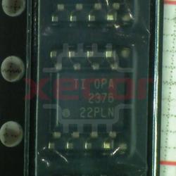
Similar Product
OPA376AIDBVR
High-performance operational amplifier
OPA2376AIDR
Dual operational amplifier offering precision, low noise performance, and low quiescent current
OPA2376AIDGKR
High-precision, low-noise dual operational amplifier with low quiescent current, designed for applications requiring accuracy and efficiency
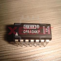
OPA404KP
Quad operational
OPA541AP
Single TO-220-11 package for ease of installation
OPA627AP
Superior performance for demanding applications
LMC6482AIM/NOPB
SMD Integrated Circuit
OPA2330AIDR
OPA2330AIDR is an op amp that contains two general-purpose channels, capable of operation within a voltage range of ±2