
MMBFJ177LT1G
Silicon-based P-channel field-effect transistor optimized for use in low-voltage electronic circuits
Inventory:5,268
- 90-day after-sales guarantee
- 365 Days Quality Guarantee
- Genuine Product Guarantee
- 7*24 hours service quarantee
-
Part Number : MMBFJ177LT1G
-
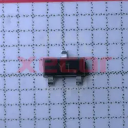
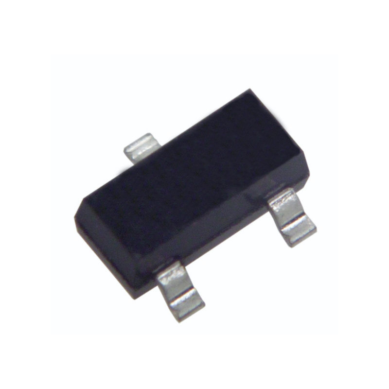
Package/Case : SOT23-3
-
Brands : Onsemi
-
Components Categories : JFETs
-
Datesheet : MMBFJ177LT1G DataSheet (PDF)
The MMBFJ177LT1G is a small-signal N-channel junction field-effect transistor (JFET) designed for low-power amplification and switching applications. This transistor features a low ON-state resistance and high forward transfer admittance, making it suitable for various analog and digital circuits. (Note: The pin configuration below is a general representation. Refer to the specific datasheet for precise details.) Incorporate a circuit diagram illustrating the connections and operation of the MMBFJ177LT1G transistor for a visual representation. Note: For detailed technical specifications, please refer to the MMBFJ177LT1G datasheet. Functionality The MMBFJ177LT1G is a small-signal N-channel JFET transistor designed for amplification and switching tasks in various electronic circuits. It provides efficient amplification with low noise and consumes minimal power, making it suitable for a wide range of applications. Usage Guide Q: What is the maximum power dissipation of the MMBFJ177LT1G? Q: Is the MMBFJ177LT1G suitable for high-frequency applications? For similar functionalities, consider these alternatives to the MMBFJ177LT1G:Overview of MMBFJ177LT1G
Pinout
Circuit Diagram
Key Features
Application
Frequently Asked Questions
A: The maximum power dissipation of the MMBFJ177LT1G is typically specified in the datasheet and depends on the operating conditions.
A: While the MMBFJ177LT1G can operate at moderately high frequencies, it is primarily designed for low-power and small-signal applications. For high-frequency applications, consider alternative transistors optimized for such purposes.Equivalent
Specifications
The followings are basic parameters of the part selected concerning the characteristics of the part and categories it belongs to.
| Status | Active | Compliance | PbAHP |
| Package Type | SOT-23-3 | Case Outline | 318-08 |
| MSL Type | 1 | MSL Temp (°C) | 260 |
| Container Type | REEL | Container Qty. | 3000 |
| ON Target | N | Channel Polarity | P-Channel |
| IDSS Min (µA) | 1500 | IDSS Max (µA) | 20000 |
| V(BR)GSS Min (V) | 30 | Ciss Max (pF) | 11 |
| Crss Max (pF) | 5.5 | Pricing ($/Unit) | $0.0828Sample |
Warranty & Returns
Warranty, Returns, and Additional Information
-
QA & Return Policy
Parts Quality Guarantee: 365 days
Returns for refund: within 90 days
Returns for Exchange: within 90 days
-
Shipping and Package
Shipping:For example, FedEx, SF, UPS, or DHL.UPS, or DHL.
Parts Packaging Guarantee: Featuring 100% ESD anti-static protection, our packaging incorporates high toughness and superior buffering capabilities.
-
Payment
For example, channels like VISA, MasterCard, UnionPay, Western Union, PayPal, and more.
If you have specific payment channel preferences or requirements, please get in touch with our sales team for assistance.
Similar Product

MMDT5451-7-F
Trans GP BJT NPN/PNP 160V 0.2A 320mW 6-Pin SOT-363 T/R

MMUN2214LT1G
SOT-23 T/R Trans Digital BJT NPN 50V 100mA 400mW

MMBT3904WT1G
The MMBT3904WT1G is a NPN-type Bipolar Transistor, ideal for applications requiring current levels of up to 200mA and voltage ratings of 60V

MMBT2222AWT1G
150mW Power Dissipation
MMSS8050-H-TP
Trans GP BJT NPN 25V 1.5A 300mW 3-Pin SOT-23 T/R

MMBTA42-TP
Trans GP BJT NPN 300V 0.3A 300mW 3-Pin SOT-23 T/R
MMBT5962
versatile NPN amplifier
MMBT3906K
Trans GP BJT PNP 40V 0.2A 350mW 3-Pin SOT-23 T/R