
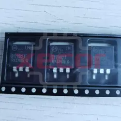
LM27222SD/NOPB
Driver 4.5A 2-OUT High and Low Side Inv/Non-Inv 8-Pin WSON EP T/R
Inventory:2,877
- 90-day after-sales guarantee
- 365 Days Quality Guarantee
- Genuine Product Guarantee
- 7*24 hours service quarantee
-
Part Number : LM27222SD/NOPB
-
Package/Case : WSON (NGT)-8
-
Brands : Texas Instruments
-
Components Categories : Gate Drivers
-
Datesheet : LM27222SD/NOPB DataSheet (PDF)
Overview of LM27222SD/NOPB
The LM27222 is a dual N-channel MOSFET driver designed to drive MOSFETs in push-pull configurations as typically used in synchronous buck regulators. The LM27222 takes the PWM output from a controller and provides the proper timing and drive levels to the power stage MOSFETs. Adaptive shoot-through protection prevents damaging and efficiency reducing shoot-through currents, thus ensuring a robust design capable of being used with nearly any MOSFET. The adaptive shoot-through protection circuitry also reduces the dead time down to as low as 10ns, ensuring the highest operating efficiency. The peak sourcing and sinking current for each driver of the LM27222 is about 3A and 4.5Amps respectively with a Vgs of 5V. System performance is also enhanced by keeping propagation delays down to 8ns. Efficiency is once again improved at all load currents by supporting synchronous, non-synchronous, and diode emulation modes through the LEN pin. The minimum output pulse width realized at the output of the MOSFETs is as low as 30ns. This enables high operating frequencies at very high conversion ratios in buck regulator designs. To support low power states in notebook systems, the LM27222 draws only 5µA from the 5V rail when the IN and LEN inputs are low or floating.
Key Features
- Adaptive Shoot-through Protection
- 10ns Dead Time
- 8ns Propagation Delay
- 30ns Minimum On-time
- 0.4Ω Pull-down and 0.9Ω Pull-up Drivers
- 4.5A Peak Driving Current
- MOSFET Tolerant Design
- 5µA Quiescent Current
- 30V Maximum Input Voltage in Buck Configuration
- 4V to 6.85V Operating Voltage
- SOIC-8 and WSON Packages
All trademarks are the property of their respective owners.
Specifications
The followings are basic parameters of the part selected concerning the characteristics of the part and categories it belongs to.
| Bus voltage (max) (V) | 30 | Power switch | MOSFET |
| Input VCC (min) (V) | 4 | Input VCC (max) (V) | 6.85 |
| Peak output current (A) | 4.5 | Operating temperature range (°C) | -40 to 125 |
| Rating | Catalog | Propagation delay time (µs) | 0.008 |
| Rise time (ns) | 17 | Fall time (ns) | 14 |
| Iq (mA) | 0.54 | Input threshold | CMOS |
| Channel input logic | CMOS | Negative voltage handling at HS pin (V) | -0.3 |
| Driver configuration | Single |
Warranty & Returns
Warranty, Returns, and Additional Information
-
QA & Return Policy
Parts Quality Guarantee: 365 days
Returns for refund: within 90 days
Returns for Exchange: within 90 days
-
Shipping and Package
Shipping:For example, FedEx, SF, UPS, or DHL.UPS, or DHL.
Parts Packaging Guarantee: Featuring 100% ESD anti-static protection, our packaging incorporates high toughness and superior buffering capabilities.
-
Payment
For example, channels like VISA, MasterCard, UnionPay, Western Union, PayPal, and more.
If you have specific payment channel preferences or requirements, please get in touch with our sales team for assistance.
Similar Product
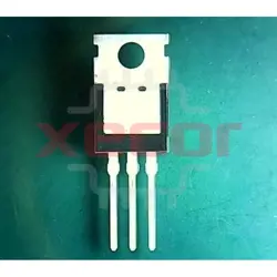
LM317AHVT
This product, LM317AHVT, is a linear voltage regulator capable of regulating positive voltage with adjustable settings using its three terminals
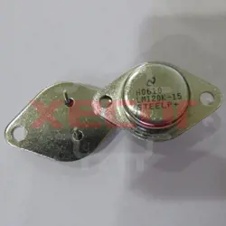
LM120K-15
5V Fixed Negative Standard Regulator BIPolar
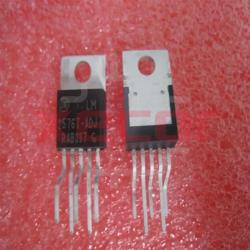
LM2576T-ADJG
3A output capability
LM1117IMP-ADJ
LDO Voltage Regulators
LM2576SX-ADJ
Switching Voltage Regulators

LM3526M-L
Hi Side Dual 5.5V 1.2A 8-Pin SOIC Tube
LM317BD2T
Linear Voltage Regulators 1.5A ADJ 1.2-37V

LM4041AIM3-1.2
V-Ref Precision 1.225V 12mA 3-Pin SOT-23 T/R