
LF353N/NOPB
FET Input Amplifiers with 5mV, 4MHz, and 50pA specifications
Inventory:5,667
- 90-day after-sales guarantee
- 365 Days Quality Guarantee
- Genuine Product Guarantee
- 7*24 hours service quarantee
-
Part Number : LF353N/NOPB
-
Package/Case : PDIP (P)-8
-
Brands : TI
-
Components Categories : AmplifiersInstrumentation, OP Amps, Buffer Amps
-
Datesheet : LF353N/NOPB DataSheet (PDF)
Overview of LF353N/NOPB
The LF353N/NOPB is a high-performance, dual operational amplifier with JFET input designed for a wide range of applications. It features low input offset voltage, a high slew rate, and low input bias current, making it ideal for precision and high-speed circuits. The LF353N/NOPB has a wide operating voltage range of ±18V and a unity gain bandwidth of 4 MHz. It also has a high open-loop gain of 106 dB and low harmonic distortion, making it suitable for audio applications.The LF353N/NOPB comes in an 8-pin PDIP package and operates over a temperature range of -40°C to 105°C. It is designed to be used in various applications such as audio amplifiers, active filters, instrumentation amplifiers, and precision voltage regulators. With its high-performance features and versatile applications, the LF353N/NOPB is a popular choice for designers looking for a reliable and efficient operational amplifier solution
Key Features
Application
Specifications
The followings are basic parameters of the part selected concerning the characteristics of the part and categories it belongs to.
| Number of channels | 2 | Total supply voltage (+5 V = 5, ±5 V = 10) (max) (V) | 36 |
| Total supply voltage (+5 V = 5, ±5 V = 10) (min) (V) | 10 | Rail-to-rail | In to V+ |
| GBW (typ) (MHz) | 4 | Slew rate (typ) (V/µs) | 13 |
| Vos (offset voltage at 25°C) (max) (mV) | 10 | Iq per channel (typ) (mA) | 1.8 |
| Vn at 1 kHz (typ) (nV√Hz) | 16 | Rating | Catalog |
| Operating temperature range (°C) | 0 to 70 | Offset drift (typ) (µV/°C) | 10 |
| Input bias current (max) (pA) | 200 | CMRR (typ) (dB) | 100 |
| Iout (typ) (A) | 0.02 | Architecture | FET |
| Input common mode headroom (to negative supply) (typ) (V) | 3 | Input common mode headroom (to positive supply) (typ) (V) | 0 |
| Output swing headroom (to negative supply) (typ) (V) | 1.5 | Output swing headroom (to positive supply) (typ) (V) | -1.5 |
Warranty & Returns
Warranty, Returns, and Additional Information
-
QA & Return Policy
Parts Quality Guarantee: 365 days
Returns for refund: within 90 days
Returns for Exchange: within 90 days
-
Shipping and Package
Shipping:For example, FedEx, SF, UPS, or DHL.UPS, or DHL.
Parts Packaging Guarantee: Featuring 100% ESD anti-static protection, our packaging incorporates high toughness and superior buffering capabilities.
-
Payment
For example, channels like VISA, MasterCard, UnionPay, Western Union, PayPal, and more.
If you have specific payment channel preferences or requirements, please get in touch with our sales team for assistance.
Similar Product
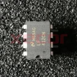
LF412CN
±18V supply voltage
LF412MH
Op Amp Dual High Speed Amplifier ±18V 8-Pin TO-99
LF356H
Op Amp Single GP ±18V 8-Pin TO-99 Box
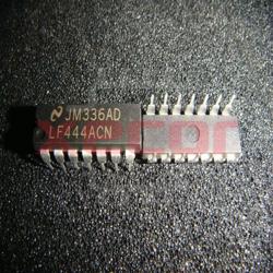
LF444ACN
Operational Amplifiers - Op Amps Quad Low Power JFET Input Operational Amplifier 14-PDIP 0 to 70
LF444CMX/NOPB
JFET Input Operational Amplifier in Quad Configuration
LF356N/NOPB
Low-power single JFET operational amplifier
LF411CP
Op Amp Single High Speed Amplifier ±18V 8-Pin PDIP Tube
LF442ACN
Precision Amplifiers Dual Low Power JFET Input Operational Amplifier 8-PDIP 0 to 70