
FDG6301N
Trans MOSFET N-CH 25V 0.22A 6-Pin SC-88 T/R
| Quantity | Unit Price(USD) | Ext. Price |
|---|---|---|
| 5 | $0.184 | $0.92 |
| 50 | $0.149 | $7.45 |
| 150 | $0.133 | $19.95 |
| 500 | $0.115 | $57.50 |
| 3000 | $0.096 | $288.00 |
| 6000 | $0.091 | $546.00 |
Inventory:5,783
- 90-day after-sales guarantee
- 365 Days Quality Guarantee
- Genuine Product Guarantee
- 7*24 hours service quarantee
-
Part Number : FDG6301N
-
Package/Case : SC70-6
-
Brands : onsemi
-
Components Categories : FET, MOSFET Arrays
-
Datesheet : FDG6301N DataSheet (PDF)
Overview of FDG6301N
These dual N-Channel logic level enhancement mode field effect transistors are produced using a proprietary, high cell density, DMOS technology. This very high density process is especially tailored to minimize on-state resistance. This device has been designed especially for low voltage applications as a replacement for bipolar digital transistors and small signal MOSFETS.
Key Features
- 25 V, 0.22 A continuous, 0.65 A Peak.
- RDS(ON) = 4 Ω @ VGS= 4.5 V,
- RDS(ON) = 5 Ω @ VGS= 2.7 V.
- Very low level gate drive requirements allowing direct operation in 3 V circuits (VGS(th) <1.5 V).
- Gate-Source Zener for ESD ruggedness (>6kV Human Body Model).
- Compact industry standard SC70-6 surface mount package.
Application
- This product is general usage and suitable for many different applications.
Specifications
The followings are basic parameters of the part selected concerning the characteristics of the part and categories it belongs to.
| Product Category | MOSFET | RoHS | Details |
| Technology | Si | Mounting Style | SMD/SMT |
| Package / Case | SOT-323-6 | Transistor Polarity | N-Channel |
| Number of Channels | 2 Channel | Vds - Drain-Source Breakdown Voltage | 25 V |
| Id - Continuous Drain Current | 220 mA | Rds On - Drain-Source Resistance | 4 Ohms |
| Vgs - Gate-Source Voltage | - 8 V, + 8 V | Vgs th - Gate-Source Threshold Voltage | 650 mV |
| Qg - Gate Charge | 400 pC | Minimum Operating Temperature | - 55 C |
| Maximum Operating Temperature | + 150 C | Pd - Power Dissipation | 300 mW |
| Channel Mode | Enhancement | Series | FDG6301N |
| Brand | onsemi / Fairchild | Configuration | Dual |
| Fall Time | 4.5 ns | Forward Transconductance - Min | 0.2 S |
| Height | 1.1 mm | Length | 2 mm |
| Product | MOSFET Small Signals | Product Type | MOSFET |
| Rise Time | 4.5 ns | Factory Pack Quantity | 3000 |
| Subcategory | MOSFETs | Transistor Type | 2 N-Channel |
| Type | FET | Typical Turn-Off Delay Time | 4 ns |
| Typical Turn-On Delay Time | 5 ns | Width | 1.25 mm |
| Part # Aliases | FDG6301N_NL | Unit Weight | 0.000988 oz |
Warranty & Returns
Warranty, Returns, and Additional Information
-
QA & Return Policy
Parts Quality Guarantee: 365 days
Returns for refund: within 90 days
Returns for Exchange: within 90 days
-
Shipping and Package
Shipping:For example, FedEx, SF, UPS, or DHL.UPS, or DHL.
Parts Packaging Guarantee: Featuring 100% ESD anti-static protection, our packaging incorporates high toughness and superior buffering capabilities.
-
Payment
For example, channels like VISA, MasterCard, UnionPay, Western Union, PayPal, and more.
If you have specific payment channel preferences or requirements, please get in touch with our sales team for assistance.
Similar Product

FDC3535
FDC3535 MOSFET with PowerTrench design, -80V rating

FDW2520C
MOSFET FDW2520C PowerTrench

FDPF7N50U
Trans MOSFET N-CH 500V 5A 3-Pin(3+Tab) TO-220F Rail

FDPF10N60NZ
Sold in a tube containing 1000 units for bulk purchasing options

DMP4047LFDE-7
Product DMP4047LFDE-7 is a P Channel MOSFET with a voltage rating of 40V and a current rating of 3.3A

IPW65R080CFD
Explore the advanced capabilities of the IPW65R080CFD, an N-Channel MOSFET Transistor
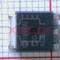
FDD4685
channel power field effect transistor, 8.4A, 40V, 0.042ohm, mosfet
FDC6561AN
MOSFET SSOT-6 N-CH 30V