
DS90CR286AMTD
LVDS Interface IC +3.3V Rising Edge Data Strobe LVDS 28-Bit Channel Link Receiver - 66 MHz 56-TSSOP -40 to 85
| Quantity | Unit Price(USD) | Ext. Price |
|---|---|---|
| 1 | $7.079 | $7.08 |
| 200 | $2.740 | $548.00 |
| 500 | $2.644 | $1,322.00 |
| 1000 | $2.596 | $2,596.00 |
Inventory:7,709
- 90-day after-sales guarantee
- 365 Days Quality Guarantee
- Genuine Product Guarantee
- 7*24 hours service quarantee
-
Part Number : DS90CR286AMTD
-
Package/Case : TSSOP-56
-
Brands : TI
-
Components Categories : Specialized
-
Datesheet : DS90CR286AMTD DataSheet (PDF)
Overview of DS90CR286AMTD
The DS90CR286A receiver converts the four LVDS data streams back into parallel 28 bits of LVCMOS data. Also available is the DS90CR216A receiver that converts the three LVDS data streams back into parallel 21 bits of LVCMOS data. The outputs of both receivers strobe on the rising edge.
The receiver LVDS clock operates at rates from 20 to 66 MHz. The device phase-locks to the input clock, samples the serial bit streams at the LVDS data lines, and converts them into parallel output data. At an incoming clock rate of 66 MHz, each LVDS input line is running at a bit rate of 462 Mbps, resulting in a maximum throughput of 1.848 Gbps for the DS90CR286A and 1.386 Gbps for the DS90CR216A.
The DS90CR286A and DS90CR216A devices are enhanced over prior generation receivers and provide a wider data valid time on the receiver output. The use of these serial link devices is ideal for solving EMI and cable size problems associated with transmitting data over wide, high speed parallel LVCMOS interfaces. Both devices are offered in TSSOP packages.
Key Features
- 20 to 66 MHz Shift Clock Support
- 50% Duty Cycle on Receiver Output Clock
- Best–in–Class Set and Hold Times on Rx Outputs
- Rx Power Consumption < 270 mW (Typ) at 66
MHz Worst Case - Rx Power-Down Mode < 200 µW (Max)
- ESD Rating > 7 kV (HBM), > 700 V (EIAJ)
- PLL Requires No External Components
- Compatible with TIA/EIA-644 LVDS Standard
- Low Profile 56-Pin or 48-Pin DGG (TSSOP)
Package - Operating Temperature: −40°C to 85°C
- Automotive Q Grade Available – AEC-Q100 Grade
3 Qualified
Specifications
The followings are basic parameters of the part selected concerning the characteristics of the part and categories it belongs to.
| Protocols | Catalog | Rating | Catalog |
| Operating temperature range (°C) | -40 to 85 |
Warranty & Returns
Warranty, Returns, and Additional Information
-
QA & Return Policy
Parts Quality Guarantee: 365 days
Returns for refund: within 90 days
Returns for Exchange: within 90 days
-
Shipping and Package
Shipping:For example, FedEx, SF, UPS, or DHL.UPS, or DHL.
Parts Packaging Guarantee: Featuring 100% ESD anti-static protection, our packaging incorporates high toughness and superior buffering capabilities.
-
Payment
For example, channels like VISA, MasterCard, UnionPay, Western Union, PayPal, and more.
If you have specific payment channel preferences or requirements, please get in touch with our sales team for assistance.
Similar Product
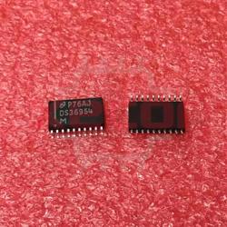
DS36954M
This product serves as a four-channel differential bus transceiver, housed in a 20-SOIC package with a temperature range of 0 to 70 degrees Celsius
SN65LVDS4RSER
High-Frequency Radio Frequency Component
DS26LS32MJ/883
Trusted supplier
DS8921AM/NOPB
Versatile SOIC-8 IC for serial communication protocols RS-485 and RS-422."
DS92LV010ATM/NOPB
LVDS signal transmission device in SOIC-8 packaging
SN65LVDS1DBVR
LVDS Driver with 0.454V Output Voltage
DS90LV001TMX
8-pin LVDS buffer designed for signal buffering and distribution in high-speed applications
DS75176BM
RS-422/RS-485 Interface IC Multipt RS-485/ RS-422 Tnscvr