
DAC121S101WGRLV
DAC 1-CH Resistor-String 12-bit 10-Pin CSOIC Tray
Inventory:8,084
- 90-day after-sales guarantee
- 365 Days Quality Guarantee
- Genuine Product Guarantee
- 7*24 hours service quarantee
-
Part Number : DAC121S101WGRLV
-
Package/Case : 10-CFP
-
Brands : TI
-
Components Categories : Digital to Analog Converters (DAC)
-
Datesheet : DAC121S101WGRLV DataSheet (PDF)
Overview of DAC121S101WGRLV
The DAC121S101QML-SP device is a full-featured, general-purpose, 12-bit voltage-output digital-to-analog converter (DAC) that can operate from a single 2.7-V to 5.5-V supply and consumes just 177 µA of current at 3.6 V. The on-chip output amplifier allows rail-to-rail output swing and the three-wire serial interface operates at clock rates up to 20 MHz over the specified supply voltage range and is compatible with standard SPI, QSPI, MICROWIRE, and DSP interfaces.
The supply voltage for the DAC121S101QML-SP serves as its voltage reference, providing the widest possible output dynamic range. A power-on reset circuit ensures that the DAC output powers up to zero volts and remains there until there is a valid write to the device. A power-down feature reduces power consumption to less than a microWatt.
The low power consumption and small packages of the DAC121S101QML-SP make it an excellent choice for use in battery-operated equipment.
Key Features
- 5962R07726
- Total Ionizing Dose 100 krad(Si)
- Single Event Latch-up Immune 120 MeV-cm2/mg
- Single Event Functional Interrupt Immune 120 MeV-cm2/mg (See Radiation Report)
- Ensured Monotonicity
- Low Power Operation
- Rail-to-Rail Voltage Output
- Power-On Reset to Zero Volts Output
- SYNC Interrupt Facility
- Wide Power Supply Range (2.7 V to 5.5 V)
- Small Packages
- Power-Down Feature
- Key Specifications
- Resolution: 12 Bits
- DNL: +0.21, –0.10 LSB (Typical)
- Output Settling Time: 12.5 µs (Typical)
- Zero Code Error: 2.1 mV (Typical)
- Full-Scale Error: –0.04% FS (Typical)
- Power Dissipation
- Normal Mode: 0.52 mW (3.6 V) and 1.19 mW (5.5 V) Typical
- Power-Down Mode: 0.014 µW (3.6 V) and 0.033 µW (5.5 V) Typical
Specifications
The followings are basic parameters of the part selected concerning the characteristics of the part and categories it belongs to.
| Source Content uid | DAC121S101WGRLV | Pbfree Code | Yes |
| Rohs Code | No | Part Life Cycle Code | Active |
| Ihs Manufacturer | TEXAS INSTRUMENTS INC | Package Description | SOP, |
| Reach Compliance Code | not_compliant | ECCN Code | 9A515.E.1 |
| HTS Code | 8542.39.00.01 | Samacsys Manufacturer | Texas Instruments |
| Converter Type | D/A CONVERTER | Input Bit Code | BINARY |
| Input Format | SERIAL | JESD-30 Code | R-CDSO-G10 |
| JESD-609 Code | e0 | Length | 6.86 mm |
| Linearity Error-Max (EL) | 0.1953% | Moisture Sensitivity Level | 1 |
| Number of Bits | 12 | Number of Functions | 1 |
| Number of Terminals | 10 | Operating Temperature-Max | 125 °C |
| Operating Temperature-Min | -55 °C | Package Body Material | CERAMIC, METAL-SEALED COFIRED |
| Package Code | SOP | Package Shape | RECTANGULAR |
| Package Style | SMALL OUTLINE | Sample Rate | 1.8 MHz |
| Seated Height-Max | 2.33 mm | Settling Time-Max | 12.5 µs |
| Settling Time-Nom (tstl) | 12.5 µs | Supply Voltage-Nom | 3 V |
| Surface Mount | YES | Technology | CMOS |
| Temperature Grade | MILITARY | Terminal Finish | TIN LEAD |
| Terminal Form | GULL WING | Terminal Pitch | 1.27 mm |
| Terminal Position | DUAL | Total Dose | 100k Rad(Si) V |
| Width | 6.12 mm |
Warranty & Returns
Warranty, Returns, and Additional Information
-
QA & Return Policy
Parts Quality Guarantee: 365 days
Returns for refund: within 90 days
Returns for Exchange: within 90 days
-
Shipping and Package
Shipping:For example, FedEx, SF, UPS, or DHL.UPS, or DHL.
Parts Packaging Guarantee: Featuring 100% ESD anti-static protection, our packaging incorporates high toughness and superior buffering capabilities.
-
Payment
For example, channels like VISA, MasterCard, UnionPay, Western Union, PayPal, and more.
If you have specific payment channel preferences or requirements, please get in touch with our sales team for assistance.
Similar Product
DAC7611P
DAC 1-CH R-2R 12-bit 8-Pin PDIP Tube
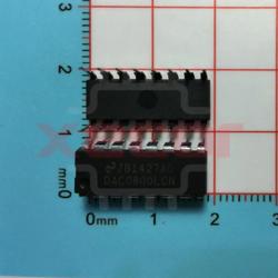
DAC0800LCN
DAC 1-CH R-2R 8-bit 16-Pin PDIP Tube
DAC081C081CIMK/NOPB
DAC 1-CH Resistor-String 8-bit 6-Pin TSOT-23 T/R
DAC7311IDCKR
DAC 1-CH Resistor-String 12-bit 6-Pin SC-70 T/R
DAC7541AKP
Digital to Analog Converters - DAC 12-Bit CMOS 4-Quad Multiplying Cnvtr
DAC0800LCN/NOPB
DAC 1-CH R-2R 8-bit 16-Pin PDIP Tube
DAC088S085CIMTX/NOPB
DAC 8-CH Resistor-String 8-bit 16-Pin TSSOP T/R
DAC121S101WGRQV
DAC 1-CH Resistor-String 12-bit 10-Pin CSOIC Tray