
AOD2916
Trans MOSFET N-CH 100V 25A 3-Pin(2+Tab) DPAK
| Quantity | Unit Price(USD) | Ext. Price |
|---|---|---|
| 1 | $0.511 | $0.51 |
| 10 | $0.417 | $4.17 |
| 30 | $0.370 | $11.10 |
| 100 | $0.324 | $32.40 |
| 500 | $0.296 | $148.00 |
| 1000 | $0.282 | $282.00 |
Inventory:4,808
- 90-day after-sales guarantee
- 365 Days Quality Guarantee
- Genuine Product Guarantee
- 7*24 hours service quarantee
-
Part Number : AOD2916
-
Package/Case : TO252-2
-
Brands : ALPHA AND OMEGA SEMICONDUCTOR
-
Components Categories : Single FETs, MOSFETs
-
Datesheet : AOD2916 DataSheet (PDF)
The AOD2916 is a N-channel Power MOSFET designed for high power applications.This MOSFET features a low on-resistance and high switching speed,making it ideal for power management in various electronic circuits. (Note:The pin configuration below is a general representation.Refer to the specific datasheet for precise details.) Include a circuit diagram illustrating the connections and operation of the AOD2916 MOSFET for a visual representation. Note:For detailed technical specifications,please refer to the AOD2916 datasheet. Functionality The AOD2916 N-channel Power MOSFET is designed for high power handling,low on-resistance,and fast switching speed,making it a reliable component for power management and control in electronic systems. Usage Guide Q: Is the AOD2916 suitable for high-frequency applications? For similar functionalities, consider these alternatives to the AOD2916:Overview of AOD2916
Pinout
Circuit Diagram
Key Features
Application
Frequently Asked Questions
A: Yes, the AOD2916 offers fast switching speeds, making it suitable for high-frequency switching circuits.Equivalent
Specifications
The followings are basic parameters of the part selected concerning the characteristics of the part and categories it belongs to.
| ECCN (US) | EAR99 | Part Status | Obsolete |
| SVHC | Yes | SVHC Exceeds Threshold | Yes |
| Automotive | No | PPAP | No |
| Category | Power MOSFET | Configuration | Single |
| Process Technology | TMOS | Channel Mode | Enhancement |
| Channel Type | N | Number of Elements per Chip | 1 |
| Maximum Drain Source Voltage (V) | 100 | Maximum Gate Source Voltage (V) | ±20 |
| Maximum Gate Threshold Voltage (V) | 2.7 | Maximum Continuous Drain Current (A) | 25 |
| Maximum Gate Source Leakage Current (nA) | 100 | Maximum IDSS (uA) | 1 |
| Maximum Drain Source Resistance (mOhm) | 34@10V | Typical Gate Charge @ Vgs (nC) | 12.5@10V|[email protected] |
| Typical Gate Charge @ 10V (nC) | 12.5 | Typical Input Capacitance @ Vds (pF) | 870@50V |
| Maximum Power Dissipation (mW) | 50000 | Typical Fall Time (ns) | 5.5 |
| Typical Rise Time (ns) | 3.5 | Typical Turn-Off Delay Time (ns) | 23 |
| Typical Turn-On Delay Time (ns) | 7.5 | Minimum Operating Temperature (°C) | -55 |
| Maximum Operating Temperature (°C) | 175 | Typical Drain Source Resistance @ 25°C (mOhm) | 28@10V|[email protected] |
| Mounting | Surface Mount | Package Height | 2.29 |
| Package Width | 6.1 | Package Length | 6.6 |
| PCB changed | 2 | Tab | Tab |
| Standard Package Name | TO-252 | Supplier Package | DPAK |
| Pin Count | 3 |
Warranty & Returns
Warranty, Returns, and Additional Information
-
QA & Return Policy
Parts Quality Guarantee: 365 days
Returns for refund: within 90 days
Returns for Exchange: within 90 days
-
Shipping and Package
Shipping:For example, FedEx, SF, UPS, or DHL.UPS, or DHL.
Parts Packaging Guarantee: Featuring 100% ESD anti-static protection, our packaging incorporates high toughness and superior buffering capabilities.
-
Payment
For example, channels like VISA, MasterCard, UnionPay, Western Union, PayPal, and more.
If you have specific payment channel preferences or requirements, please get in touch with our sales team for assistance.
Similar Product

AO4407A
ROHS compliant SOP-8 MOSFETs
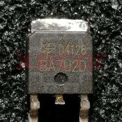
AOD4126
Trans MOSFET N-CH 100V 43A 3-Pin(2+Tab) DPAK
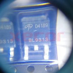
AOD4189
Trans MOSFET P-CH 40V 40A 3-Pin(2+Tab) DPAK

AON7403
Power Field-Effect Transistor with 29A I(D)

AO4882
N-channel MOSFET transistor designed for switching applications

AOD417
P-channel 30-volt, 25-ampere transistor with a three-pin DPAK package
AO4485
Trans MOSFET P-CH 40V 10A 8-Pin SOIC T/R

AOD407
Trans MOSFET P-CH 60V 12A 3-Pin(2+Tab) DPAK T/R