
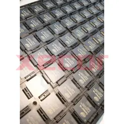
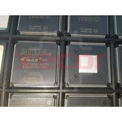
10M02SCE144C8G
Product 10M02SCE144C8G
| Quantity | Unit Price(USD) | Ext. Price |
|---|---|---|
| 1 | $9.013 | $9.01 |
| 10 | $7.867 | $78.67 |
| 60 | $7.169 | $430.14 |
| 120 | $6.582 | $789.84 |
Inventory:4,155
- 90-day after-sales guarantee
- 365 Days Quality Guarantee
- Genuine Product Guarantee
- 7*24 hours service quarantee
-
Part Number : 10M02SCE144C8G
-
Package/Case : EQFP-144
-
Brands : Intel
-
Components Categories : FPGAs (Field Programmable Gate Array)
-
Datesheet : 10M02SCE144C8G DataSheet (PDF)
The 10M02SCE144C8G is a low-cost, low-power field-programmable gate array (FPGA) featuring 1152 LUTs (Look-Up Tables) and 10,000 logic elements. This FPGA offers versatile programmable logic capabilities for various digital design applications. (Note: The pin configuration below is a general representation. Refer to the specific datasheet for precise details.) Include a circuit diagram illustrating the connections and operation of the 10M02SCE144C8G FPGA for a visual representation. Note: For detailed technical specifications, please refer to the 10M02SCE144C8G datasheet. Functionality The 10M02SCE144C8G FPGA offers reprogrammable logic resources that can be tailored to specific project requirements. It enables designers to create custom digital circuits efficiently and cost-effectively. Usage Guide Q: Can the 10M02SCE144C8G be reprogrammed multiple times? Q: What software tools are recommended for programming this FPGA? For similar functionalities, consider these alternatives to the 10M02SCE144C8G:Overview of 10M02SCE144C8G
Pinout
Circuit Diagram
Key Features
Application
Frequently Asked Questions
A: Yes, the 10M02SCE144C8G FPGA supports multiple reprogramming cycles, allowing flexibility in design iterations.
A: Popular FPGA development tools like Quartus Prime and Vivado are commonly used for programming and configuring the 10M02SCE144C8G.Equivalent
Specifications
The followings are basic parameters of the part selected concerning the characteristics of the part and categories it belongs to.
| Product Category | FPGA - Field Programmable Gate Array | RoHS | Details |
| Series | MAX 10 10M02 | Number of Logic Elements | 2000 LE |
| Embedded Memory | 108 kbit | Number of I/Os | 101 I/O |
| Supply Voltage - Min | 2.85 V | Supply Voltage - Max | 3.465 V |
| Minimum Operating Temperature | 0 C | Maximum Operating Temperature | + 85 C |
| Mounting Style | SMD/SMT | Package / Case | EQFP-144 |
| Brand | Altera | Maximum Operating Frequency | 450 MHz |
| Moisture Sensitive | Yes | Number of Logic Array Blocks - LABs | 125 LAB |
| Operating Supply Voltage | 3 V, 3.3 V | Product Type | FPGA - Field Programmable Gate Array |
| Factory Pack Quantity | 60 | Subcategory | Programmable Logic ICs |
| Tradename | MAX | Part # Aliases | 965251 |
| Unit Weight | 0.321581 oz |
Warranty & Returns
Warranty, Returns, and Additional Information
-
QA & Return Policy
Parts Quality Guarantee: 365 days
Returns for refund: within 90 days
Returns for Exchange: within 90 days
-
Shipping and Package
Shipping:For example, FedEx, SF, UPS, or DHL.UPS, or DHL.
Parts Packaging Guarantee: Featuring 100% ESD anti-static protection, our packaging incorporates high toughness and superior buffering capabilities.
-
Payment
For example, channels like VISA, MasterCard, UnionPay, Western Union, PayPal, and more.
If you have specific payment channel preferences or requirements, please get in touch with our sales team for assistance.
Similar Product
10CL010YU256C8G
Suppliers for Original Equipment Manufacturers and Contract Manufacturers only
10CL025YU256I7G
256UBGA IC FPGA with 150 I/o
EPM240T100I5
The EPM240T100I5 CPLD provides engineers with a powerful and efficient solution for designing complex digital systems
EPM570T100I5N
This programmable logic device is suitable for CPLDs and FPGAs
10M50SAE144I7G
5nm Technology EP Tray
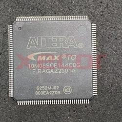
10M08SCE144C8G
144EQFP, FPGA - Field Programmable Gate Array non-volatile FPGA, 101 I/O
10M08SCU169I7G
Twenty-pin SOIC IC with multiple D-type latches and tri-state functionality
10M02SCE144I7G
Low power consumption and high performance