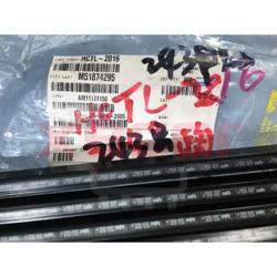
74LS00 Pinout, Datasheet, Truth Table, and Uses
 Prof. David Reynolds
Published:March 13, 2024
Digital logic gates are electronic devices that perform logical operations on binary inputs to produce a binary output. They are the building blocks of digital circuits, enabling the creation of complex logical functions and operations. NAND gates are one of the basic types of logic gates and are widely used in digital circuit design. They produce a high output (1) only when both inputs are low (0), making them versatile for implementing various logical functions. The 74LS00 is a well-known and fundamental gate from the logic gate family, which includes AND, OR, and NOT gates. Each gate has a distinct internal circuit and serves different purposes in devices. By combining these gates, we can create other gates such as NAND, NOR, XOR, and XNOR. These gates can be constructed using transistors, resistors, and capacitors. However, the size of a single gate can become larger than expected when these circuits are created. In this comprehensive guide, we'll take a deep dive into the 74LS00 pinout, circuit, datasheet, uses, and more details. Everything you need to know about this quad 2 input NAND gate.

What is 74LS00?
The 74LS00 is a TTL (Transistor transistor-to-transistor logic) IC that utilizes low-power Schottky transistors to reduce stored charge and achieve higher switching speeds compared to conventional bipolar transistors. It is part of the 74XXYY IC series, which consists of logic gates used in digital electronics. The 74LS00 IC contains four NAND gates, each with two inputs, hence its name "QUAD TWO INPUT NAND GATE."
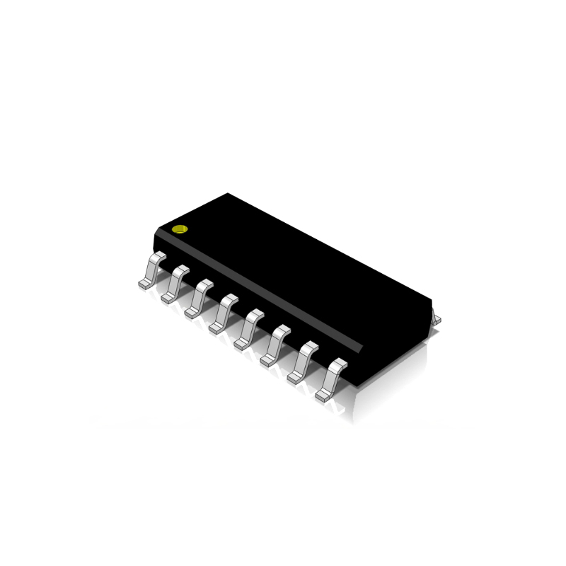
Being NAND gates-based, the 74LS00 IC is versatile and can be easily converted into OR and NOT gates. It features 14 pins, all connected to the four NAND gates. The IC is available in three packages: SOIC, PDIP, and SOP.
74LS00 Pinout
The 74LS00 is a 14-pin device available in various packages chosen based on requirements. Descriptions for each pin are provided below.

74LS00 Pin Diagram
74LS00 Pin Configuration
| Pin No. | Pin Name | Description |
| NAND GATE 1 | ||
| 1 | A1 | Pin 1 will be the input of the first NAND gate in IC 74LS00. |
| 2 | B1 | Pin 2 will be used as the second Input of First NAND gate. |
| 3 | Y1 | The output of the first NAND gate will be available at Pin 3. |
| NAND GATE 2 | ||
| 4 | A2 | Pin 4 will be used for the input of the second NAND gate. |
| 5 | B2 | The second input of the second NAND gate will be given at Pin 5. |
| 6 | Y2 | The output of the second NAND gate will be available at Pin 6. |
| NAND GATE 3 | ||
| 9 | A3 | Pin 9 will be used as the first input pin for the third NAND gate. |
| 10 | B3 | Pin 10 will be the second input of the third NAND gate. |
| 8 | Y3 | Third NAND gate output will be at Pin 8. |
| NAND GATE 4 | ||
| 12 | A4 | Pin 12 will be used for the first input of the 4th NAND gate. |
| 13 | B4 | The second input of the fourth NAND gate will be at Pin 13. |
| 11 | Y4 | The output of the fourth NAND gate will available at Pin 11. |
| SHARED TERMINALS | ||
| 7 | GND | Pin 7 will be used at the common ground by devices and the power supply that will use with 74LS00. |
| 14 | Vcc | Pin 14 will be used to give power to the IC. |
Features of 74LS00
- Available in various packages, including SOIC, PDIP, and SOP.
- Suitable for use in high-frequency systems.
- It can function as a NAND gate and is easily convertible into other gates due to the NAND gate's universality.
- Outputs TTL signals due to its internal TTL-based structure.
74LS00 Specifications
| Type | Parameter |
| Operating Voltage Range | +4.75 to +5.25V |
| Maximum Supply Voltage | 7V |
| Maximum Output Current per Gate | 8mA |
| Output Type | TTL |
| Maximum ESD | 3.5KV |
| Typical Rise Time | 15ns |
| Typical Fall Time | 15ns |
| Operating Temperature Range | 0°C to 75°C |
| Pack/Case | SOIC, PDIP, and SOP. |
74LS00 Equivalent/Alternative
The 74LS00, a quad 2-input NAND gate, has several equivalents that offer similar functionality and performance. These equivalents include:
74HC00 (High-speed CMOS): The 74HC00 is a high-speed CMOS quad 2-input NAND gate that can be used as an equivalent to the 74LS00. It offers high speed and low power consumption.
74HCT00 (High-speed CMOS, TTL compatible): The 74HCT00 is a high-speed CMOS quad 2-input NAND gate that is compatible with TTL logic levels. It can be used as a drop-in replacement for the 74LS00 in TTL applications.
SN54LS00: The SN54LS00 is part of the 54LS00 series, a series of low-power Schottky TTL integrated circuits. It is functionally equivalent to the 74LS00.
SN7400: The SN7400 is part of the 7400 series, a series of TTL integrated circuits. It is functionally equivalent to the 74LS00.
CD4011: The CD4011 is a CMOS quad 2-input NAND gate that can be used as an equivalent to the 74LS00. It offers low power consumption and high noise immunity.
74LVC00 (Low Voltage TTL): The 74LVC00 is a low voltage TTL quad 2-input NAND gate that can be used as an equivalent to the 74LS00. It operates at a lower voltage and offers compatibility with TTL logic levels.
74AC00 (Advanced CMOS): The 74AC00 is an advanced CMOS quad 2-input NAND gate that can be used as an equivalent to the 74LS00. It offers high speed and low power consumption.
74ALS00 (Advanced Low-Power Schottky TTL): The 74ALS00 is an advanced low-power Schottky TTL quad 2-input NAND gate that can be used as an equivalent to the 74LS00. It offers low power consumption and high speed.
74F00 (Very High Speed): The 74F00 is a very high-speed TTL quad 2-input NAND gate that can be used as an equivalent to the 74LS00. It offers very high-speed operation.
74C00 (CMOS, similar to the 4000-series): The 74C00 is a CMOS quad 2-input NAND gate that is similar to the 4000-series of CMOS integrated circuits. It can be used as an equivalent to the 74LS00.
74LS00 CAD Model

74LS00 2 input NAND Gate Working Principle
The 74LS00 IC contains four NAND gates, each with two internal structures: CMOS and PMOS. While their physical appearance may differ, their primary function remains the same. The CMOS NAND gate comprises four transistors, creating a complex circuit that produces HIGH and LOW states based on different input combinations.
Here’s the internal structure of the NAND gate:

The internal structure includes VDD as the Power input, A and B as the Logic inputs, and Y as the Output. The transistors (Q1, Q2, Q3, Q4) ensure that when a single input is HIGH, the output should be HIGH, but due to Q3 and Q4, the output is inverted. This configuration of transistors forms the NAND gate circuit. The input always determines the output of logic gates.
| INPUT | OUTPUT | |
| A | B | Y |
| 0 | 0 | 1 |
| 0 | 1 | 1 |
| 1 | 0 | 1 |
| 1 | 1 | 0 |
Thus, each NAND gate in this IC follows a specific truth table, producing a LOW state on the output when the input is HIGH, and vice versa.
Where to Use it & How to Use
The 74LS00 is commonly used in electronic circuits for several reasons. Here are a few examples of its applications:
- NAND Function: The 74LS00's primary use is performing the NAND function. With four NAND gates in a single IC, each gate can be utilized independently.
- Logic Inverter: The NAND gates can be reconfigured to function as NOT gates, providing a total of four NOT gates within the chip if needed.
- High-Speed NAND Operation: The 74LS00 is ideal for applications requiring high-speed NAND operations. Its low transition times make it suitable for use in high-frequency systems.
- Cost-Effectiveness: This IC is one of the most affordable options available, making it widely popular and easily accessible.
As previously mentioned, the 74LS00 IC contains four NAND gates. The internal connection of these four gates is illustrated below.

A NAND gate is essentially a combination of an AND gate and a NOT gate, expressed as NAND = AND + NOT. The truth table for a NAND gate is as follows:
74LS00 Truth Table
| Input1 | Input2 | AND Output | NAND Output |
| Low | Low | Low | High |
| High | Low | Low | High |
| Low | High | Low | High |
| High | High | High | Low |
To understand the responses of a NAND gate, let's examine its internal circuitry:

1. When both inputs A1 and B1 are LOW:
- Both transistors Q1 and Q2 will be OFF.
- The total supply voltage appears across transistors Q1 and Q2, making output Y1 HIGH.
2. When any one input is HIGH:
- Only the respective transistor will be ON, leaving the other OFF.
- The entire supply voltage appears across the transistor that is OFF.
- Output Y1 will be HIGH.
3. When both inputs are HIGH:
- Both transistors will be ON, causing the voltage across both of them to be zero.
- Output Y1 will be LOW.
After examining these cases, we can see that they satisfy the truth table for a NAND gate. The output equation for a NAND gate is given as Y = AB.
Now, let's consider a simple application circuit using the NAND gate of the 74LS00 chip:

Two inputs are connected to two buttons, and the output is connected to an LED. The ON and OFF states of this LED can determine the logic state of the output gate.
- When both buttons are not pressed (open), both inputs of the gate will be LOW, resulting in a HIGH output. The LED will turn ON.
- If one button is closed, one input will be LOW, and the other will be HIGH. The output will still be HIGH, causing the LED to remain ON.
- Only when both buttons are pressed will both inputs be HIGH, resulting in a LOW output and turning the LED OFF.
By utilizing all four gates in this manner, we can effectively use the 74LS00 NAND gates to fulfill our requirements.
74LS00 Circuit Example
Here are three examples designed using a 74LS00 8-bit 2-input quad NAND gate IC.
The NAND gate is a universal gate that can be easily converted to other gates. To convert the NAND gate to an OR, NOT, or even an AND gate, specific combinations need to be followed. These combinations vary for each gate. First, let's convert the NAND gate to a NOT gate. To do this, we need to connect the first two input wires of the NAND gate. Then, we apply the input to that single input pin, effectively turning the gate into a NOT gate. Here's the representation.

To convert the NAND gate to an OR gate, we need to add two NOT gates at the input pins. We can use the NOT gate made from the NAND gate, as discussed earlier. To convert the NAND gate to an AND gate, we can use the NOT gate at the output pins to easily create an AND gate. Other gates like XOR and XNOR can also be made from the NAND gate, but this requires all four gates of the 74LS00. Here is the graphical representation of these gates.
Example in Proteus
In Proteus, we will use the IC for basic functions. We will convert all four gates into different types of gates. For example, one NAND gate will be converted into a NOT gate, and the others will be OR gates. To do this, first, insert the IC and then add some logic state inputs and viewers. Then, convert the first 3 NAND gates into NOT gates by connecting their input pins. Next, connect the output of two NAND gates to the input of the four NAND gates. Now, apply the input to the first gate, and you will get the inverted outputs.

When you apply the logic to the other circuits, the results will be as expected.

Using the IC is straightforward, and it is readily available due to its widespread use. The only concern when using the IC is voltage protection, as high voltages can affect it. Here, we only use the IC to create two types of gates, but it can be used for more complex designs as well.
74LS00 Applications
- General-purpose logic: The 74LS00 is widely used in general-purpose logic circuits, where it performs basic logic functions such as AND, OR, and NOT operations. Its simple design and reliability make it suitable for a wide range of applications.
- Digital electronics: In digital electronics, the 74LS00 is used to design and build digital circuits such as counters, shift registers, and multiplexers. Its high-speed operation and compatibility with TTL logic levels make it a popular choice for digital circuitry.
- PCs and notebooks: The 74LS00 is used in PCs and notebooks for various purposes, including interfacing with peripherals, data processing, and control logic. Its low cost and availability make it an ideal component for use in consumer electronics.
- Servers: In servers, the 74LS00 is used for tasks such as data processing, memory management, and input/output control. Its high-speed operation and reliability are crucial for the efficient operation of servers in data centers and other environments.
- Arithmetic logic units (ALUs): The 74LS00 is used in ALUs, which are essential components of processors. ALUs perform arithmetic and logic operations on binary numbers, and the 74LS00 is used to implement the basic logic functions required for these operations.
- Networking: In networking equipment, the 74LS00 is used for tasks such as packet switching, routing, and data processing. Its high-speed operation and compatibility with TTL logic levels make it suitable for use in networking applications.
- Digital systems: The 74LS00 is used in various digital systems, including industrial control systems, automation systems, and embedded systems. Its reliability and compatibility with TTL logic levels make it a popular choice for these applications.
74LS00 Advantages
- The IC includes four NAND gates, each capable of serving a distinct gate function.
- Since the NAND gate can be transformed into a NOT gate by rearranging the pins, the 74LS00 can be used as an inverter.
- Being one of the most cost-effective integrated circuits, the 74LS00 is more popular than other ICs.
- It can perform high-speed NAND operations in nanoseconds without requiring the assistance of a microcontroller or processor.
74LS00 Package

74LS00 Datasheet
Download 74LS00 Datasheet PDF.
74LS00 vs. 74HC00
The 74HC00 and 74LS00 are both ICs featuring four basic NAND gates, which are fundamental in digital electronics. The key difference lies in their speed characteristics, with the 74HC00 being high-speed and the 74LS00 being low-speed.
Here are some other differences between the two ICs:
| Feature | 74LS00 | 74HC00 |
| Supported Voltage | Limited to 5V | 2V to 6V |
| Output Current (5V) |
HIGH-Level Output Current: 0.4 mA; LOW-Level Output Current: 8 mA |
4 mA (sink or source) |
| Logic Levels | Standard TTL logic, 2.0 V@5Vcc for logic 1 | Hi logic level requires minimum 3.5 V@5Vcc |
| Output Drive | Higher output drive capability | - |
| Input Loading | Higher input loading | - |
| Speeds and Delays | Faster speeds, shorter delays | - |
| Compatibility | Not directly compatible due to differences in voltage levels and drive | Pin-compatible with 74LS00, but not directly compatible due to differences |
The HC family was designed to match the speed of the LS while consuming lower power, achieved through CMOS technology.
Conclusion
The 74LS00 Quad 2 Input NAND Gate has played a significant role in the evolution of digital electronics. Its simplicity, reliability, and versatility have made it a cornerstone in the design of digital circuits. From basic logic gates to complex processors, the 74LS00 has been a go-to component for engineers and hobbyists alike. Future developments of the 74LS00 may focus on increasing speed, reducing power consumption, and integrating more functionality into smaller packages.
Read More
FAQ
-
Is 74LS00 a NAND gate?
The 74LS00 IC is a Quad 2 Input NAND Gate.
-
How many pins are in 74LS00?
14 pins.
-
What is the input voltage of 74LS00?
4.75V to 5.25V.
-
How much power does 74LS00 use?
2.4ma typical, 4.4ma max.
-
What is the difference between 74LS00 and 7400?
The 74LS00 family offers technical improvements over the 7400 family in two main aspects: faster speed and lower power consumption. However, the 74LS00 family's limitation compared to the 7400 family is that it can only source half as much current.
-
What does 74 mean in IC?
The "74" designation indicates that the IC is a commercial-grade member of the family.


Still, need help? Contact Us: [email protected]